
The rules and standard for designing a good PCB stack-up
The rules and standards for designing a good stack-up are hundreds. Let’s just see a few:
- Ground plane boards are better because they allow signal routing in a microstrip or strip-line configuration. It also significantly reduces the ground impedance and, therefore, the ground noise;
- High speed signals should be “routed” on intermediate layers located between the various levels. In this way, ground planes can act as a shield and contain the radiation coming from the tracks at high speed;
- The signal layers should be very close to each other, even in adjacent planes.
- A signal layer must always be adjacent to a plane;
- Multiple ground planes are very advantageous, since they lower the board’s ground impedance and reduce radiation in a common way;
- The power and mass planes must be rigorously coupled together;

To achieve all these objectives, it is necessary to operate with a minimum of eight layers. Moreover:
- From a mechanical point of view, it is advisable to implement a cross section to avoid deformations;
- Configurations should be symmetric. For example, on an eight-layer PCB, if level 2 is a plane, level 7 should also be a plane;
- If the signal levels are next to the levels of the plane (ground or power) the return current can flow on an adjacent plane reducing the inductance of the return path to a minimum;
- To further improve noise and EMI performance, insulation between a signal layer and its adjacent plane can be made even thinner;
- An important consideration to be made is the thickness of each signal layer. There are standard thicknesses together with the properties of different types of printed circuit material. When selecting the materials, it is advisable to consider their electrical, mechanical and thermal properties;
- Use excellent software to help you design your stack-up. All this should be done in order to choose the correct materials from the library and perform impedance calculations based on the materials and their dimensions.
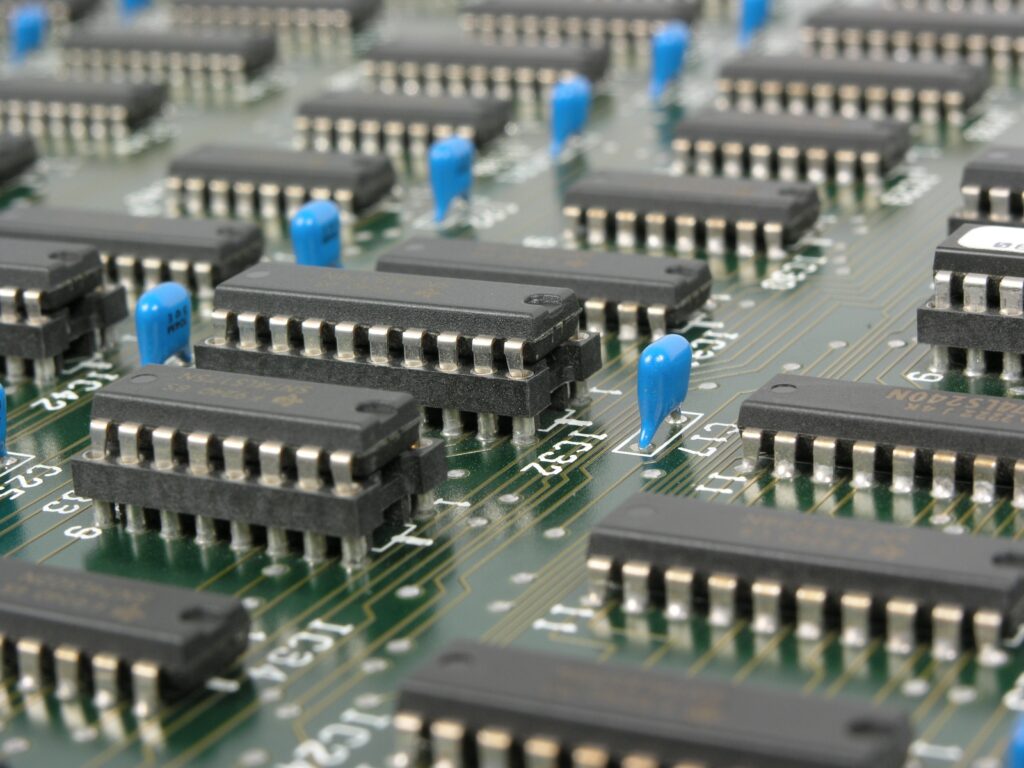
Careful PCB design is necessary
At the high operating speeds of today’s circuits, careful PCB design is necessary, and it is becoming, in all respects, an art. A poorly designed printed circuit board can degrade the electrical performance of signal transmission, power delivery, producibility and long-term reliability of the finished product.
The sending of Gerber files to companies determines the production costs, which, as with any other goods, are lowered according to the required quantities. The global growth of the PCBs market is driven by the increased use of multilayer, flexible PCBs. The board density and design complexity keep increasing as electronic companies try to add more features to the devices. Price, quality, delivery time and service are the most common criteria for choosing a PCB manufacturer, and most people should be concerned about the price first.
Proto-Electronics’ mission is to help you in this crucial prototyping phase by cutting your lead times. Online quotes in 10 minutes and delivery lead times starting from 5 working days will give you more peace of mind to work.
