

In order to properly design the multilayer PCB, it’s should carefully consider the design of the layer stack-up. For example a multilayer PCB with 4 layers is said to have 4 layers of copper either it is Ground or Power plane or Signal layer. Usually the conductive copper layer is pre-impregnated upon and below the FR-4 glass fiber sheet then another pre-preg layer is covered upon and below the stack and then another copper layer is covered on top and bottom and so on.
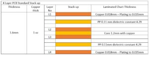
Up-to 4 layers of PCB the single core is good, but for more layers like for 6 layers there should be 2 cores and for 8 layers there should be 3 cores. The layers are always taken in even numbers for purpose of uniformity in layer stack.
The multi-layer PCB is the combination of two or more single or double sided PCBs hence a strong mutual connection is in between. The increasing complexity of multilayer PCB give rise to some typical issues that are noise, signal interference, cross talk, stray capacitances and impedance mismatch. These issues are needed to be professionally handled otherwise the overall PCB performance and reliability can greatly shatter.
A properly designed layer stack up can help reduce circuit’s vulnerability to Electromagnetic Interference (EMI) and external noises that can distort high speed signals. A good layer stack up also helps to avoid cross talks, improves signal integrity and impedance matching can reduce power losses. The perfect layer stack can also reduce cost of manufacturing of multilayer PCB.
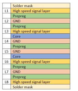
The multilayer stack up will enable you to place more circuitry on the limited space while diverting your routing to internal signal layers by means of blind and buried via. The separate ground GND and power PWR planes are used which are also copper layers.
The layer stack up should be symmetrical and the minimum clearance between traces, layers spacing, and the thickness of core should be carefully taken. The thickness of core can be from 0.1mm to 0.3mm.
The base substrate core material FR-4 is pre-impregnated with epoxy resin system. The pre-preg is use as the adhesive to form the laminated stack of these multiple layers. This is done by lamination machine that works under high temperature and pressure.
What is Multilayer PCB Stack-up?
A stack-up is the arrangement of layers of copper and insulators that make up a PCB before designing the final layout of the board. Managing a good stack-up is not exactly easy and companies that make multilayer printed circuits such as Proto-Electronics, a platform dedicated to the rapid prototyping of SMT printed circuits and cross-section components, for professionals, must be at the forefront.
Having multiple layers increases the board’s ability to distribute energy, reduces cross-interference, eliminates electromagnetic interference and supports high-speed signals. While a stack-up level allows you to get multiple electronic circuits on a single board through the various layers of PCB board, the structure of the PCB stack-up design provides many other advantages:
- A stack of PCB layers can help minimize the circuit vulnerability to external noise, as well as minimize radiation and decrease impedance and crosstalk problems on high-speed systems;
- A good PCB stacking can also contribute to efficient and low-cost final production;
- A correct stack of PCB layers can improve the electromagnetic compatibility of the project.
With a single-layer or double-layer PCB the board thickness is rarely considered. However, with the advent of multilayer PCBs, the pile of materials is starting to become more and more critical and the final cost is the factor that affects the entire project. The simplest stack-ups can include 4-layer PCBs, up to the more complex ones that require professional sequential lamination. The higher the number of layers, the more the designer is free to unravel his circuit, with less chance of stumbling into “impossible” solutions. The PCB overlapping operations consist in the arrangement of the copper layers and the insulating layers that make up a circuit. The stack-up you choose certainly plays an important role in the performance of the board in several ways.
For example, good layering can reduce the impedance of the board and limit radiation and crosstalk. It also has a major impact on the EMC performance of a product. On the other hand, poor stack-up design can significantly increase circuit radiation and noise. There are four important factors to consider when dealing with board stack-up:
- Number of Layers
- The number and types of plans used (power plans and ground plans);
- Sorting and sequence of levels;
- Spacing between levels.
Usually, not much consideration is given to these factors, except for those affecting the number of layers. Often the fourth factor is not even known to the PCB designer. When deciding on the number of layers, you need to consider the following:
- The number of signals to be routed and their cost;
- Operating frequency;
- Whether the product will meet Class A or Class B emission requirements;
- Whether the PCB will be in a shielded container or not;
- Whether the design team is competent on EMC rules and regulations.
All factors are important and critical and should be considered equally. Multilayer boards that use mass and power plane provide a significant reduction in radiated emissions. A rule of thumb, which is often used, is that a four-layer board will produce 15 dB less radiation than a two-layer board, all other factors being equal.