Wingate

Industrial PCB Repair in Malaysia

Industrial PCB Repair in Malaysia: Complete Guide to PCB Diagnosis and Repair

Industrial electronic equipment depends on reliable printed circuit boards (PCBs) to control machines, automation systems, production lines, and critical processes. When an industrial PCB fails, replacing the entire equipment is not always the most practical or cost-effective solution.

Industrial PCB repair can restore a faulty circuit board, extend the service life of equipment, and provide an alternative when the original PCB is obsolete or no longer available.

For companies looking for PCB repair in Malaysia, Wingate Electronic provides industrial PCB inspection, diagnosis, component-level repair, testing, and PCB reverse engineering services for a wide range of industrial electronic boards.

What Is Industrial PCB Repair?

Industrial PCB repair is the process of diagnosing and repairing a faulty printed circuit board used in industrial equipment and automation systems.

Unlike simply replacing a damaged component, professional PCB repair normally involves a systematic process to identify the actual cause of failure.

Depending on the condition of the board, the repair process may include:

  • Visual inspection
  • Electrical testing
  • Power supply testing
  • Component testing
  • Short-circuit and open-circuit checks
  • PCB track and via inspection
  • IC and semiconductor testing
  • Component replacement
  • Damaged PCB trace repair
  • Connector replacement
  • Corrosion cleaning and repair
  • Functional testing
  • Final inspection

The objective is not simply to replace a failed component, but to determine why the PCB failed and whether the board can be safely returned to service.

Industrial PCB Repair in Malaysia

Why Repair an Industrial PCB Instead of Replacing It?

Replacing an industrial PCB can be difficult, particularly when the equipment is old, discontinued, or supplied by a manufacturer that no longer supports the model.

PCB repair may provide several advantages.

1. Reduce Equipment Downtime

A failed control board can stop an entire machine or production process.

Repairing the existing board may be faster than waiting for an obsolete replacement board to be sourced.

2. Reduce Replacement Costs

For older industrial equipment, a replacement PCB may be expensive or difficult to obtain.

A professional industrial PCB repair service can provide an alternative by repairing the existing board.

3. Support Obsolete Equipment

Many factories continue using reliable machinery for many years.

However, the electronic boards inside these machines may become obsolete.

When the original PCB is no longer manufactured, repair and reverse engineering may be possible options.

4. Preserve Existing Equipment

If the mechanical system, software and machine are still functioning correctly, replacing the entire machine simply because of a failed PCB may not be necessary.

A successful PCB repair can help extend the useful life of the equipment.

Common Industrial PCB Problems

Industrial PCBs can fail for many different reasons. The visible damage is not always the actual cause of the failure.

Some common problems include:

Burnt Components

Overvoltage, short circuits, excessive current or component failure can cause resistors, capacitors, diodes, transistors and other components to burn.

A burnt component should not simply be replaced without investigating the underlying cause.

Failed Power Supply Section

Power supply circuits are one of the common areas associated with PCB failure.

Problems may involve:

  • Fuses
  • Rectifiers
  • Switching power supplies
  • MOSFETs
  • Voltage regulators
  • Capacitors
  • Transformers
  • Protection circuits

A failure in the power section can prevent the entire board from operating.

Damaged PCB Tracks

Excessive current, overheating or physical damage can burn or break copper tracks.

These damaged tracks may sometimes be repaired depending on the extent and location of the damage.

Corrosion and Moisture Damage

Industrial equipment can operate in environments exposed to humidity, dust, chemicals and moisture.

Corrosion can affect:

  • Copper tracks
  • Connectors
  • Component terminals
  • IC pins
  • Solder joints
  • Vias

The longer corrosion remains untreated, the greater the risk of permanent PCB damage.

Failed ICs and Microcontrollers

Industrial control boards may contain microcontrollers, memory ICs, communication ICs, drivers and other specialised integrated circuits.

When these components fail, diagnosis can be more complicated because the board may require additional testing or reverse engineering.

Connector and Terminal Damage

Repeated connection and disconnection, vibration, mechanical stress or incorrect wiring can damage PCB connectors and terminals.

Intermittent Faults

Some industrial PCBs do not fail completely.

Instead, the equipment may experience:

  • Random shutdown
  • Intermittent alarms
  • Unstable operation
  • Communication errors
  • Unexpected resets
  • Machine stopping after running for a period of time

Intermittent faults can be particularly difficult to diagnose because the PCB may appear to operate normally during a basic inspection.

How Industrial PCB Repair Is Performed

A professional PCB repair process should be systematic rather than based on replacing components randomly.

At Wingate Electronic, an industrial PCB can typically go through the following process.

Step 1: Initial PCB Inspection

The board is first inspected for visible signs of damage.

This may include:

  • Burn marks
  • Cracked components
  • Missing components
  • Corrosion
  • Damaged connectors
  • Broken tracks
  • Poor solder joints
  • Previous repair work
  • Signs of overheating

Photographs and inspection records can also be used to document the board’s condition before repair.

Step 2: Electrical and Component Testing

The PCB is then tested to identify abnormal readings and possible failure areas.

Depending on the board, testing may include:

  • Resistance measurements
  • Continuity testing
  • Diode testing
  • Voltage measurements
  • Power rail testing
  • Component-level testing
  • Short-circuit checks

The exact diagnostic method depends on the PCB design and failure symptoms.

Step 3: Fault Diagnosis

The test results are analysed to identify the likely cause of failure.

This is an important stage because replacing a visibly damaged component does not necessarily solve the original problem.

For example, a burnt transistor may have failed because another component in the circuit caused excessive current.

Step 4: Component-Level Repair

Where repair is technically feasible, faulty components may be replaced.

Depending on the PCB, this can include:

  • Resistors
  • Capacitors
  • Diodes
  • Transistors
  • MOSFETs
  • Voltage regulators
  • Relays
  • ICs
  • Connectors
  • Other electronic components

The repair approach depends on the board condition, component availability and the nature of the fault.

Step 5: PCB Track and Solder Repair

Damaged copper tracks, solder joints and other PCB-level problems may also be repaired where technically possible.

However, severely burned, delaminated or physically damaged PCB areas may not always be repairable.

Step 6: Functional Testing

After repair, the board should be tested as far as practical.

Testing may include:

  • Power-up testing
  • Input/output testing
  • Communication testing
  • Signal testing
  • Functional testing
  • Comparison with known-good readings or reference boards

The objective is to verify that the repaired PCB operates correctly under the available test conditions.

Can Every Industrial PCB Be Repaired?

No.

A professional PCB repair company should assess the condition of the board before confirming that repair is possible.

Repair may be difficult or uneconomical when:

  • The PCB has severe fire damage
  • Multiple layers are extensively damaged
  • The PCB substrate is severely burned
  • Important ICs are unavailable
  • Proprietary components cannot be sourced
  • Critical firmware is damaged or unavailable
  • The board has severe corrosion
  • The PCB has extensive physical damage
  • The original circuit cannot be reliably identified

In some cases, PCB reverse engineering or PCB redesign may be considered as an alternative to direct repair.

What Information Should You Provide for PCB Repair?

Providing more information can help the repair process start faster.

When contacting a PCB repair service in Malaysia, it is useful to provide:

PCB Information

  • PCB manufacturer
  • PCB model number
  • Part number
  • Equipment model
  • Serial number, if available
  • PCB photographs

Failure Information

Explain what happened before the PCB stopped working.

For example:

The machine suddenly stopped operating.

or:

The PCB powers on but there is no output signal.

or:

The board was exposed to water.

or:

The machine shows an error after the PCB was installed.

The more information available, the easier it may be to understand the failure symptoms.

Industrial PCB Repair for Obsolete Equipment

One of the biggest challenges faced by factories is maintaining older equipment.

A machine may still be mechanically reliable while its electronic control board is no longer supported.

This creates a problem:

The machine works, but the replacement PCB is no longer available.

In such situations, several options may be considered:

  1. Repair the original PCB
  2. Source an equivalent replacement
  3. Reverse engineer the PCB
  4. Redesign the PCB
  5. Manufacture a replacement PCB

This is where PCB repair and PCB reverse engineering can work together.

If the original board can be repaired, repair may be the simplest solution.

If the board is beyond economical repair but sufficient information can be recovered, reverse engineering may provide another option for creating a replacement.

What Types of Industrial Electronics Can Be Repaired?

Industrial PCB repair can apply to many types of electronic control boards, depending on the PCB condition and availability of technical information.

Examples include:

  • PLC control boards
  • HMI control boards
  • Industrial controller boards
  • Inverter boards
  • Servo drive boards
  • Power supply boards
  • Motor control boards
  • Machine control boards
  • Automation control boards
  • Communication boards
  • I/O boards
  • Industrial electronic modules
  • Special-purpose control PCBs

Each PCB is different, so repair feasibility should be assessed individually.

Why Choose Wingate Electronic for Industrial PCB Repair?

Wingate Electronic provides industrial PCB repair, PCB inspection, PCB testing and PCB reverse engineering services for customers who need support for industrial electronic equipment.

Our approach focuses on understanding the PCB and its failure rather than simply replacing components without diagnosis.

Our services can include:

This allows customers to work with one service provider from PCB inspection and repair through to reverse engineering, PCB fabrication and assembly, where required.

Need an Industrial PCB Repaired?

If you have a faulty, damaged, obsolete or discontinued industrial PCB, send the PCB model number and clear photographs to Wingate Electronic for an initial assessment.

Where possible, please provide:

  • PCB model / part number
  • Equipment model
  • Clear photos of both sides of the PCB
  • Description of the failure
  • Error code, if available
  • Previous repair information, if any

Our team can assess the available information and determine whether the PCB is suitable for repair, reverse engineering or replacement PCB development.

Wingate Electronic — Industrial PCB Repair & Reverse Engineering Specialist

Contact us to discuss your industrial PCB repair requirements in Malaysia.

Industrial PCB Repair in Malaysia: Complete Guide to PCB Diagnosis and Repair Read More »
PCB fabrication Malaysia

Complete Guide to PCB Fabrication in Malaysia: From Design to Finished Circuit Board

Introduction

Printed Circuit Board (PCB) fabrication is one of the most important processes in modern electronics manufacturing. Almost every electronic device, from industrial automation equipment and control systems to consumer electronics, requires a reliable PCB to connect electronic components and ensure stable operation.

For companies developing new electronic products or maintaining existing industrial equipment, choosing the right PCB fabrication partner is essential to achieve good quality, reliability, and cost efficiency.

Wingate Electronic provides professional PCB fabrication services in Malaysia, supporting prototype development, small batch production, and industrial PCB manufacturing requirements.

What Is PCB Fabrication?

PCB fabrication is the process of manufacturing a printed circuit board based on a PCB design file. The fabrication process converts a PCB layout design into a physical circuit board by creating copper tracks, drilling holes, applying surface finishes, and performing quality inspections.

The main purpose of PCB fabrication is to create a reliable electrical connection between electronic components such as:

  • Microcontrollers
  • Integrated circuits (ICs)
  • Resistors and capacitors
  • Power components
  • Connectors
  • Sensors
  • Industrial automation modules

A properly fabricated PCB ensures stable electrical performance and long-term reliability.

PCB fabrication Malaysia

The PCB Fabrication Process

1. PCB Design and Engineering Review

Before manufacturing begins, the PCB design needs to be reviewed carefully.

The PCB design stage includes:

  • Circuit schematic design
  • PCB layout
  • Component placement
  • Signal routing
  • Power distribution
  • Design for Manufacturing (DFM) checking

A proper design review helps prevent manufacturing problems such as incorrect footprints, insufficient clearance, and signal interference.

2. Gerber File Preparation

The Gerber file is the standard file format used by PCB manufacturers to produce circuit boards.

Typical PCB fabrication files include:

  • Gerber files
  • Drill files
  • PCB layer information
  • Solder mask information
  • Silkscreen data
  • Board outline drawing

Accurate Gerber files are important because manufacturing errors can lead to delays and additional costs.

3. PCB Material Selection

Selecting the correct PCB material depends on the application requirements.

Common PCB materials include:

FR-4 PCB

FR-4 is the most commonly used PCB material because it provides:

  • Good electrical insulation
  • Excellent mechanical strength
  • Cost effectiveness
  • Wide application range

It is commonly used in industrial control boards, power supply boards, and electronic equipment.

High-Frequency PCB Materials

For applications requiring high-speed signals or high-frequency operation, specialised materials such as Rogers PCB may be required.

Applications include:

  • RF communication systems
  • High-frequency circuits
  • Advanced industrial equipment

4. PCB Layer Construction

PCB layers are selected based on circuit complexity.

Common PCB layer options:

  • Single-layer PCB
  • Double-layer PCB
  • Multilayer PCB

Multilayer PCBs are widely used in advanced industrial electronics because they provide:

  • Better signal integrity
  • Compact design
  • Improved power distribution

Wingate Electronic supports PCB fabrication requirements from simple boards to complex multilayer designs.

4. PCB Layer Construction

PCB layers are selected based on circuit complexity.

Common PCB layer options:

  • Single-layer PCB
  • Double-layer PCB
  • Multilayer PCB

Multilayer PCBs are widely used in advanced industrial electronics because they provide:

  • Better signal integrity
  • Compact design
  • Improved power distribution

Wingate Electronic supports PCB fabrication requirements from simple boards to complex multilayer designs.

5. Copper Etching and Circuit Formation

During fabrication, copper layers are processed to create the required circuit patterns.

The process includes:

  • Copper lamination
  • Photo imaging
  • Etching
  • Layer alignment
  • Inspection

This creates the electrical pathways needed for component connections.

6. Drilling and Plating

PCB manufacturers drill holes for:

  • Through-hole components
  • Vias
  • Connectors
  • Mechanical mounting

After drilling, copper plating is applied to ensure proper electrical connection between PCB layers.

7. Surface Finishing

Surface finishing protects exposed copper areas and improves solderability.

Common PCB surface finishes include:

HASL (Hot Air Solder Leveling)

Advantages:

  • Cost effective
  • Good solderability
  • Suitable for general applications

ENIG (Electroless Nickel Immersion Gold)

Advantages:

  • Flat surface
  • Better reliability
  • Suitable for fine-pitch components
  • Longer shelf life

The correct surface finish depends on the application and component requirements.

8. PCB Testing and Quality Inspection

Quality control is essential before PCB delivery.

Common inspection methods include:

  • Visual inspection
  • Electrical testing
  • Automated Optical Inspection (AOI)
  • Dimensional checking

Proper testing helps ensure the PCB meets customer specifications.

Factors to Consider When Choosing a PCB Fabrication Partner

1. Manufacturing Capability

A reliable PCB supplier should understand different PCB requirements, including:

  • Prototype PCB
  • Small quantity production
  • Industrial PCB
  • Custom PCB solutions

2. Quality Control

PCB quality directly affects the reliability of the final product.

Important quality factors include:

  • Accurate dimensions
  • Reliable copper thickness
  • Proper surface finishing
  • Consistent manufacturing process

3. Technical Support

A PCB fabrication partner should provide engineering support to identify potential issues before production.

Professional advice can help reduce:

  • Manufacturing problems
  • Production delays
  • Unnecessary costs

Why Choose Wingate Electronic for PCB Fabrication in Malaysia?

Wingate Electronic provides PCB fabrication solutions for industrial and electronic applications.

Our services include:

We support various PCB requirements, including:

  • FR-4 PCB
  • Multilayer PCB
  • Industrial control PCB
  • Custom electronic circuit boards

With experience in industrial electronics and automation systems, Wingate Electronic helps customers transform their electronic designs into reliable finished circuit boards.

Conclusion

PCB fabrication is a critical step in electronics manufacturing. From PCB design verification and material selection to manufacturing and testing, every process affects the final quality and reliability of the circuit board.

Choosing an experienced PCB fabrication partner can help businesses reduce production risks, improve product quality, and shorten development time.

If you require PCB fabrication, PCB assembly, PCB design, or industrial electronic repair services in Malaysia, Wingate Electronic is ready to support your project.

Contact Wingate Electronic today for your PCB fabrication requirements.

Complete Guide to PCB Fabrication in Malaysia: From Design to Finished Circuit Board Read More »

Latest PCB Technology in 2026

Latest PCB Technology in 2026 | PCB Design & Manufacturing Trends

The electronics industry is advancing at an unprecedented pace. Emerging technologies such as Artificial Intelligence (AI), Electric Vehicles (EVs), Industrial Automation, 5G communication, and the Internet of Things (IoT) are pushing Printed Circuit Board (PCB) technology to new heights. Modern electronic devices require PCBs that are smaller, faster, more reliable, and capable of handling increasingly complex designs.

As a result, PCB manufacturers are investing in innovative manufacturing techniques, advanced materials, and intelligent design tools to meet these evolving demands. This article explores the latest PCB technology trends in 2026 and how they are transforming product development across multiple industries.

1. High-Density Interconnect (HDI) PCB Technology

HDI (High-Density Interconnect) PCBs have become the preferred solution for compact, high-performance electronic products. By using microvias, blind vias, buried vias, and fine-pitch routing, HDI boards can accommodate more components within a smaller footprint.

Benefits of HDI PCBs

  • Increased component density
  • Smaller and lighter PCB designs
  • Faster signal transmission
  • Improved signal integrity
  • Reduced electromagnetic interference (EMI)
  • Enhanced product reliability

Common Applications

  • Smartphones
  • Tablets
  • Wearable devices
  • Medical equipment
  • Industrial automation
  • Consumer electronics

As electronic devices continue to shrink while offering greater functionality, HDI technology has become a standard solution for modern PCB design.


PCB Fabrication and PCB Assembly

2. High-Speed PCB Design

The increasing demand for high-speed data transmission has made signal integrity one of the most important considerations in PCB design.

High-speed PCB layouts require careful engineering to minimize signal degradation and ensure stable communication between components.

Key Design Considerations

  • Controlled impedance routing
  • Differential pair routing
  • Length matching
  • Ground plane optimization
  • Crosstalk reduction
  • Power integrity analysis

These techniques are essential for products using interfaces such as PCI Express (PCIe), USB 4.0, DDR5 memory, Ethernet, HDMI, and DisplayPort.

3. Advanced Multilayer PCB Technology

As electronic systems become more sophisticated, multilayer PCB technology continues to evolve. While four-layer and six-layer boards are still widely used, many industrial and telecommunications applications now require 12-layer, 16-layer, or even 30-layer PCBs.

Advantages

  • Higher circuit density
  • Better power distribution
  • Reduced electrical noise
  • Improved signal quality
  • Compact product design

Multilayer PCBs are commonly found in networking equipment, aerospace systems, industrial controllers, and AI servers.

4. Advanced PCB Materials

Selecting the appropriate PCB material is essential for achieving reliable electrical performance and effective thermal management.

Popular materials include:

  • FR-4
  • High-Tg FR-4
  • Rogers laminates
  • Isola materials
  • Ceramic substrates
  • Aluminum PCBs
  • Copper-core PCBs

These materials offer improved thermal conductivity, lower dielectric loss, and excellent performance in high-frequency applications.

5. Thermal Management Solutions

Modern power electronics generate significant heat, making efficient thermal management a critical aspect of PCB design.

Common thermal solutions include:

  • Thermal vias
  • Heavy copper PCBs
  • Metal Core PCBs (MCPCB)
  • Copper coin technology
  • Embedded heat spreaders

Effective heat dissipation improves product reliability, extends component lifespan, and reduces the risk of system failure.

Applications include LED lighting, power supplies, motor drives, EV charging systems, and renewable energy equipment.

6. Flexible and Rigid-Flex PCB Technology

Flexible and rigid-flex PCBs allow engineers to create lightweight, space-saving electronic products with improved mechanical reliability.

Advantages

  • Reduced wiring
  • Higher resistance to vibration
  • Lower assembly cost
  • Improved product durability
  • Compact mechanical design

These PCB technologies are widely used in aerospace, medical equipment, cameras, robotics, and wearable electronics.

7. AI-Powered PCB Design

Artificial Intelligence is revolutionizing the PCB design process by assisting engineers with faster and more accurate design decisions.

AI can optimize:

  • Component placement
  • PCB routing
  • Signal integrity analysis
  • Design rule checking
  • Manufacturing optimization

The result is shorter design cycles, lower production costs, and improved manufacturing quality.

8. Smart PCB Manufacturing

Industry 4.0 is transforming PCB manufacturing through automation, robotics, and real-time process monitoring.

Modern production lines now integrate:

  • Automated Optical Inspection (AOI)
  • Automated X-ray Inspection (AXI)
  • Flying Probe Testing
  • In-Circuit Testing (ICT)
  • Functional Circuit Testing (FCT)
  • Automated SMT Assembly

These technologies improve manufacturing accuracy, reduce defects, and ensure consistent product quality.

9. Sustainable PCB Manufacturing

Environmental responsibility is becoming increasingly important within the electronics industry.

PCB manufacturers are adopting sustainable practices such as:

  • Lead-free soldering
  • Halogen-free materials
  • Energy-efficient production
  • Water recycling systems
  • Waste reduction initiatives

These environmentally friendly processes help manufacturers comply with international standards while reducing their environmental impact.

10. The Future of PCB Technology

PCB technology will continue evolving alongside AI, autonomous systems, electric vehicles, and next-generation communication networks.

Emerging innovations include:

  • Embedded component PCBs
  • Glass substrate technology
  • Optical PCB interconnects
  • Advanced semiconductor packaging
  • 3D PCB structures
  • AI-driven manufacturing
  • Ultra-high-density PCB designs

These advancements will enable faster, more reliable, and more efficient electronic products for the future.

Why Choose Wingate Electronic?

At Wingate Electronic Sdn Bhd, we provide complete PCB solutions to support customers from prototype development to mass production.

Our Services

  • PCB Design & Schematic Capture
  • PCB Layout Design
  • PCB Fabrication
  • PCB Prototype Manufacturing
  • PCB Assembly (SMT & Through-Hole)
  • Reverse Engineering
  • Electronic Component Sourcing
  • PCB Repair & Troubleshooting
  • Functional Testing & Inspection

With years of industry experience, we deliver reliable, high-quality PCB solutions for industrial automation, medical devices, consumer electronics, telecommunications, and power electronics.

Conclusion

The latest PCB technology is driving innovation across every sector of the electronics industry. From HDI PCBs and advanced multilayer boards to AI-assisted design and smart manufacturing, these technologies enable manufacturers to build faster, smaller, and more reliable electronic products.

Whether you are developing an industrial control system, IoT device, medical instrument, or consumer electronic product, selecting the right PCB technology is essential for achieving superior performance and long-term reliability.

If you are looking for a trusted PCB manufacturer in Malaysia, Wingate Electronic provides professional PCB design, PCB fabrication, PCB assembly, and engineering support to help transform your ideas into high-quality products.

Latest PCB Technology in 2026 | PCB Design & Manufacturing Trends Read More »

Latest PCB Industry News in Asia and Malaysia (2026 Update)

The printed circuit board (PCB) industry in Asia continues to show strong momentum in 2025–2026, driven by rapid growth in electronics manufacturing, electric vehicles (EVs), data centers, and AI-related hardware. Asia remains the global backbone of PCB production, with Southeast Asia — especially Malaysia — playing an increasingly important role.

Asia Remains the Global PCB Powerhouse

China, Taiwan, South Korea, and Japan continue to dominate high-volume and high-technology PCB manufacturing. Demand for HDI PCBs, multilayer boards, and advanced packaging substrates has increased significantly due to:

  • AI servers and cloud data centers
  • Automotive electronics and EV power modules
  • 5G and industrial automation
PCB Fabrication and PCB Assembly

At the same time, many global electronics companies are diversifying their supply chains away from single-country dependence. This shift has accelerated investment into Southeast Asia, including Malaysia, Thailand, and Vietnam.

Malaysia’s Growing Role in the PCB Supply Chain

Malaysia is strengthening its position as a key electronics manufacturing hub in Asia. The country benefits from:

  • A mature E&E (Electrical & Electronics) ecosystem
  • Strong presence of multinational semiconductor and EMS companies
  • Skilled engineering workforce and stable infrastructure

In recent years, Malaysia has seen increased activity in:

  • Industrial and automotive PCBs
  • Power electronics boards for inverters, chargers, and motor control
  • High-reliability PCB assembly and repair services

Penang, Selangor, and Johor continue to attract PCB-related investments, supporting both high-mix, low-volume and mass production manufacturing.

Technology Trends Impacting Asian PCB Manufacturers

Several key technology trends are shaping the PCB landscape in Asia:

  • Power electronics PCBs: Growing demand for thick copper, high-current designs used in EVs, solar inverters, and industrial power supplies.
  • Advanced materials: Increased use of high-TG, low-loss, and thermally conductive substrates.
  • Miniaturization: Continued adoption of HDI designs, fine-pitch components, and compact layouts.
  • Socket and modular designs: More customers are requesting socket-based solutions for power devices (e.g. TO-247 packages) to allow easier replacement and testing.

Challenges and Opportunities

While demand is strong, PCB manufacturers in Asia also face challenges such as:

  • Rising material and labor costs
  • Tighter quality and reliability requirements
  • Longer lead times for certain components

However, these challenges also create opportunities for specialized PCB services, including:

  • PCB design optimization
  • Engineering support and troubleshooting
  • PCB repair, modification, and prototyping

Companies that can provide technical support, flexibility, and fast response times are well positioned to stand out in the market.

Outlook for 2026

Looking ahead, the PCB industry in Asia — particularly in Malaysia — is expected to remain resilient and competitive. Growth will continue to be driven by automotive electronics, renewable energy systems, AI infrastructure, and industrial automation.

For local PCB service providers and manufacturers, the focus in 2026 will be on quality, reliability, and value-added engineering services, rather than price alone.

Latest PCB Industry News in Asia and Malaysia (2026 Update) Read More »

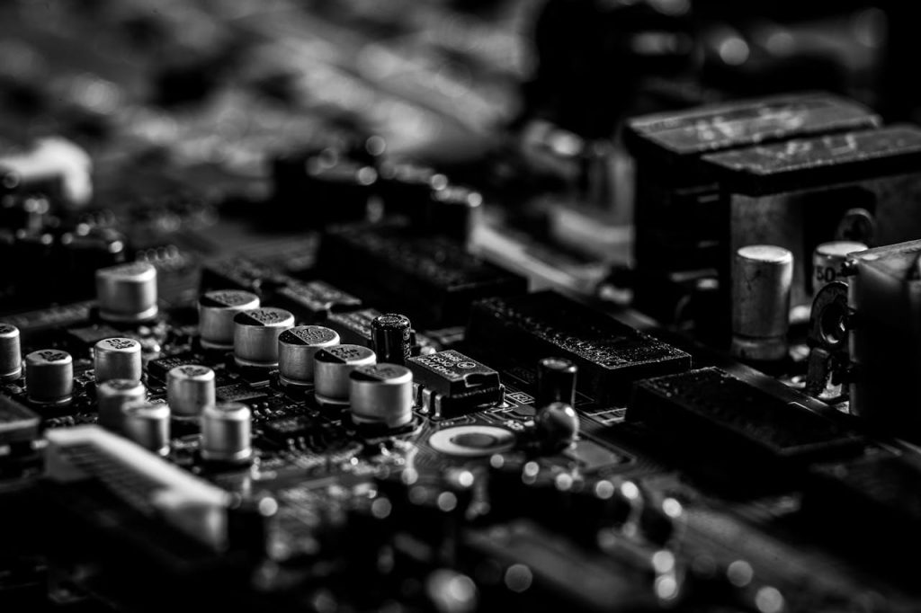
Close-up view of a printed circuit board (PCB) showing capacitors and electronic components in black and white.

Latest PCB Technology: Trends, Innovations & What’s Next

In the rapidly evolving electronics landscape, printed circuit board (PCB) technology continues to drive innovation. From high-speed communications to wearable devices, PCBs are at the heart of nearly every modern electronic product. In this article, we explore the latest trends in PCB tech, what innovations are shaping the future, and what companies/arise need to know to stay ahead.

What Has Evolves So Far

To understand the present, it helps to look back. Early PCBs were rigid, single-sided or double-sided boards using simple plated through-holes (PTH). Over time, multilayer boards, surface-mount technology (SMT), then high-density interconnect (HDI) have become standard.

More recent developments include rigid-flex boards, thicker copper plating for power applications, boards made for RF/microwave applications, and special materials (like Rogers, aluminum cores, ceramics) to meet high-frequency, high-thermal or harsh-environment requirements.

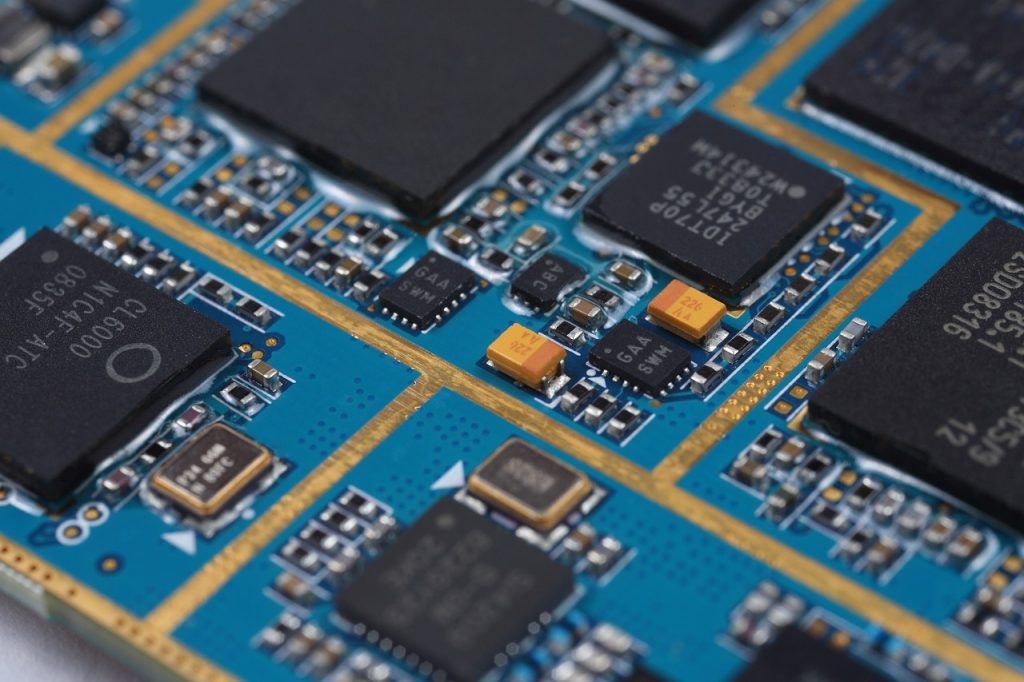
Close-up view of electronic circuit board showing components and connectors on a modern PCB.
PCB Frabrication and PCB Assembly

Key Trends & Breakthroughs in Modern PCB Technology

Here are the cutting-edge trends that are transforming PCB design, fabrication, and application:

1. High-Frequency, High-Speed PCBs

As 5G/6G, IoT, and high-speed digital electronics proliferate, demands for PCBs that support higher signal frequencies are growing. What this means: lower dielectric loss, tighter tolerances for trace width and spacing, and better material choices.

2. Multilayer & HDI (High Density Interconnect)

More layers allow more complex routing, reduce board size, and support more functionality. HDI—including buried vias, blind vias, microvias—is now essential for mobile, wearable, and compact devices.

3. Rigid-Flex & Flexible PCBs

To get around mechanical constraints, bending, or fitting PCBs into odd shapes, rigid-flex and fully flexible boards are increasingly common. They reduce connectors, save space, and often improve reliability in applications where the board must flex or fold.

4. Advanced Materials

The substrate and dielectric materials are improving: higher Tg (glass transition temperature), lower coefficient of thermal expansion (CTE), higher thermal conductivity, and materials optimized for high-frequency performance are in demand. Metal cores, ceramic bases, or hybrid materials are getting more used.

5. Embedded / Inserted Components

Embedding passive or even active components within substrate layers (rather than surface mounting everything) helps reduce size, improve electrical performance (less parasitic capacitance/inductance), and improve thermal behavior.

6. 3D Printing and Additive Manufacturing

It’s a newer area, but additive techniques for PCB production (printing conductive traces, using printable substrates, etc.) are showing potential especially for rapid prototyping or custom, low-volume production.

7. Better Imaging and Precision Techniques

Techniques such as Laser Direct Imaging (LDI) are replacing older mask-based methods. This improves resolution, reduces defects, and allows finer features needed for HDI and high-frequency boards.

8. Soldering and Assembly Innovations

Innovations in soldering (laser soldering, selective soldering), surface finishes (lead-free, ENIG, etc.), and more precise assembly help ensure reliability in smaller components, mixed technology boards, and in environments with thermal stress.

9. Sustainability / Eco-friendly PCB Solutions

Cutting down waste, reducing copper usage, using more environmentally friendly materials, and improving recyclability are rising priorities. A recent example is Elephantech’s SustainaCircuits™ technology, which aims to reduce copper usage by ~70-80% while being multilayer and rigid-substrate compatible.

Applications Driving Demand

These innovations are not happening in a vacuum. Key industries are pushing the envelope, requiring more from PCB tech:

  • Telecommunications & 5G/6G: High frequency performance, low loss, HDI, RF-specific substrates.
  • Automotive & Electric Vehicles: Thermal management, high-power handling, reliability under vibration & temperature extremes.
  • Medical & Wearables: Miniaturization, flexible/rigid-flex PCBs, biocompatibility (sometimes), high reliability.
  • Aerospace / Defense: Mission-critical reliability, extreme environment operation, often needing certifications.
  • IoT & Consumer Electronics: Compact size, low cost, flexible form factors, high speed but also mass production.
Challenges and What’s Holding Back Faster Adoption

While there’s much promise, several hurdles remain:

  • Cost: High-performance materials, specialized equipment (for microvias, LDI, flexible substrates) cost more.
  • Manufacturing complexity: As boards get more dense / multilayer / embedded parts, fabrication and assembly steps become more intricate, increasing risk of defects.
  • Reliability under stress: Thermal cycling, mechanical flex, moisture, etc., can degrade designs if not properly engineered.
  • Supply chain and materials availability: Some advanced materials are harder to source, or have long lead times.
  • Skill & design constraints: Designers must have experience with high-speed layout, signal integrity, thermal management, etc. Not all teams are ready.
What PCB Manufacturers & Designers Should Do

To stay at the cutting edge, here’s what companies and engineers should consider:

  1. Invest in new fabrication tools for microvia drilling, laser imaging, accurate multilayer lamination, rigid-flex capability.
  2. Material R&D / qualification to find substrates with better performance (thermal, electrical, mechanical) that are also cost-effective.
  3. Design for manufacturability (DfM) & Design for reliability (DfR): from the layout stage, think about how signal integrity, thermal stresses, and assembly yield will affect end product.
  4. Environmentally conscious design: reducing material waste, using recyclable materials, minimizing copper usage, considering lifecycle impacts.
  5. Collaboration & standardization: As industries (automotive, medical, telecom) require certifications and high reliability, following standards (IPC, ISO, etc.) and collaborating across the supply chain helps.
  6. Prototyping and simulation: using simulations (thermal, signal, mechanical), prototype runs, and quality testing early helps catch issues before scaling up.
What’s Coming: The Next Frontiers

Looking ahead, some of the exciting innovations likely to shape PCB technology are:

  • Printed Light Boards (PLBs): Combining lighting or optical elements directly into boards.
  • More widespread use of additive manufacturing and printed electronics, possibly even replacing copper traces in certain applications.
  • Higher layer counts and stack-ups with more complex via topologies (buried, blind, micro-vias, etc.) to pack more functions in less space.
  • Smart / adaptive PCBs: Boards that can self-monitor (temperature, stress) or adapt performance.
  • Material science breakthroughs: composites, nanomaterials, substrates with ultra-low loss for RF, better thermal dissipation.

Latest PCB Technology: Trends, Innovations & What’s Next Read More »

The Power of AI Technology

The Power of AI Technology

Design Optimization:

AI technology has transformed the electronic design process by enabling advanced optimization techniques. Designers can leverage AI algorithms to explore a vast design space, quickly evaluate numerous possibilities, and identify the most efficient and effective designs. AI algorithms can analyze design constraints, performance objectives, and historical data to generate optimized circuit layouts, improve power efficiency, reduce electromagnetic interference, and enhance overall design performance.

For example, AI-based optimization algorithms can analyze a wide range of circuit parameters and constraints to find the optimal trade-off between power consumption, performance, and cost. These algorithms can identify design solutions that human designers might overlook, leading to more efficient and innovative electronic designs.

Predictive Maintenance:

In the manufacturing phase, AI technology plays a crucial role in predictive maintenance. By continuously monitoring sensors and data points, AI algorithms can detect anomalies, predict equipment failures, and recommend preventive actions. This proactive approach minimizes unplanned downtime, reduces maintenance costs, and optimizes production efficiency.

AI-powered predictive maintenance algorithms can analyze real-time data, historical records, and equipment performance patterns to accurately forecast maintenance requirements and schedule interventions accordingly. For example, by monitoring equipment vibration, temperature, and power consumption data, AI algorithms can identify signs of impending equipment failure and alert maintenance teams to take preventive action. This ensures that equipment operates at peak performance, reduces costly downtime, and extends the lifespan of machinery.

Quality Control and Inspection:

AI technology enhances quality control and inspection processes in electronic manufacturing. Visual inspection, a critical aspect of quality control, benefits from AI-driven machine vision systems. These systems employ deep learning algorithms to analyze images and detect defects, such as soldering errors, component misalignment, or physical damage. By automating the inspection process, AI technology improves accuracy, reduces human error, and increases throughput, ultimately ensuring higher product quality.

Supply Chain Optimization:

AI technology offers immense value in optimizing the electronic manufacturing supply chain. By analyzing historical data, market trends, and demand patterns, AI algorithms can accurately forecast material requirements, manage inventory levels, and optimize procurement processes. This helps to minimize supply chain disruptions, reduce excess inventory, lower costs, and enhance overall efficiency.

AI algorithms can analyze vast amounts of data to identify patterns and correlations, enabling more accurate demand forecasting. By leveraging this information, manufacturers can optimize their production schedules, avoid stockouts, and reduce inventory carrying costs. Additionally, AI-powered algorithms can continuously monitor market trends and supplier performance, allowing manufacturers to make informed decisions regarding sourcing strategies and supplier selection.

Process Automation:

RPA can automate various tasks across the manufacturing process, such as generating production reports, updating inventory databases, or performing quality control checks.

The Power of AI Technology Read More »

SMT Soldering Quality

The Factors Affecting SMT Soldering Quality and Effective Solutions

Introduction

Solder Paste Quality:

Solder paste composition: Ensure that the solder paste is formulated to meet the specific requirements of the components and the soldering process. Consider factors such as lead-free vs. lead solder, flux type, and activity level.

Viscosity: Monitor and control the viscosity of the solder paste to ensure consistent and uniform deposition. Use viscosity measurement tools and adjust the paste or the printing process parameters accordingly.

Particle size distribution: Solder paste with a well-controlled particle size distribution provides better stencil release and improves solder paste printing quality. Regularly check the particle size distribution using laser diffraction or similar methods.

Soldering Temperature Profile:

Preheat: Ensure that the preheating phase brings the PCB and components to the desired temperature gradually, avoiding thermal shock and potential component damage.

Soak: Maintain a stable temperature during the soak phase to allow the flux to activate fully and promote proper wetting.

Reflow: Optimize the reflow profile by adjusting the ramp rate, peak temperature, and cooling rate to achieve the right balance between solder joint formation and minimizing thermal stress on the components.

Component Placement Accuracy:

Vision systems: Utilize advanced pick-and-place machines equipped with vision systems to align and orient components accurately. These systems can detect variations in component position, rotation, or polarity, reducing the likelihood of misalignment.

Calibration and maintenance: Regularly calibrate the placement machines to ensure precision and accuracy. Maintain and clean the nozzles, feeders, and placement heads to prevent any debris or misalignment issues.

Automated Optical Inspection (AOI): Implement AOI systems to detect and flag any component placement errors. This allows for immediate corrective actions, reducing the chances of soldering defects.

PCB Design Considerations:

Pad design: Optimize the pad geometry, including pad size, shape, and solder mask relief, to ensure sufficient solder wetting and proper solder joint formation.

Stencil design: Collaborate with stencil manufacturers to design stencils that provide consistent and accurate solder paste deposition, taking into account the component footprint and recommended solder paste volume.

Solder mask clearance: Maintain appropriate solder mask clearance around pads to avoid solder bridging and ensure proper solder joint formation.

Operator Training and Skills:

Comprehensive training programs: Develop training programs that cover the fundamentals of soldering, equipment operation, process parameters, and quality standards. Provide hands-on training to enhance the operators’ skills in component handling, solder paste application, and reflow techniques.

Continuous improvement: Encourage operators to stay updated with the latest industry trends and advancements through workshops, seminars, and certifications. Foster a culture of continuous learning and improvement within the organization.

Conclusion

The Factors Affecting SMT Soldering Quality and Effective Solutions Read More »

High Temperature and Humidity on PCB Performance

Unveiling the Effects of High Temperature and Humidity on PCB Performance

Introduction

Printed circuit boards (PCBs) are integral components in electronic devices, serving as the foundation for interconnecting and powering various electronic components. As electronic devices continue to advance, it becomes crucial to understand the environmental factors that can affect the performance and reliability of PCBs. In this article, we will explore the impact of high temperature and humidity on PCBs, shedding light on potential challenges and necessary precautions.

The Effects of High Temperature

  1. Thermal Stress: High temperatures can subject PCBs to thermal stress, which may lead to component failure or solder joint degradation. Excessive heat can cause expansion and contraction of the board and its components, potentially resulting in mechanical and electrical failures.
  2. Material Integrity: Elevated temperatures can adversely affect the material integrity of PCBs. The substrate material, typically made of fiberglass-reinforced epoxy, may experience thermal degradation, compromising the structural strength of the board.
  3. Signal Integrity: High temperatures can impact the electrical properties of the PCB, leading to signal integrity issues. Heat-induced expansion and contraction can alter the impedance characteristics of transmission lines, causing signal distortions or reflections.
  4. Component Performance: Electronic components on the PCB, such as integrated circuits (ICs), capacitors, and resistors, often have specified operating temperature ranges. Operating beyond these temperature limits can affect their performance, reliability, and even lifespan.

The Effects of High Humidity

  1. Corrosion: High humidity levels can create a conducive environment for the formation of moisture on the PCB surface. Moisture, in the presence of oxygen, can lead to corrosion of the conductive traces, solder joints, and component leads, compromising the electrical connectivity.
  2. Conductive Contamination: Humidity can contribute to the accumulation of conductive contaminants, such as dust, salts, or other pollutants, on the PCB surface. These contaminants can cause short circuits or interfere with signal transmission, leading to malfunction or reduced performance.
  3. Insulation Breakdown: Excessive humidity can deteriorate the insulation properties of PCB materials, such as solder mask or conformal coating. This breakdown may result in leakage currents, reduced insulation resistance, or even insulation failure.

Precautions and Mitigation Strategies

To mitigate the adverse effects of high temperature and humidity on PCBs, several precautions can be taken:

  1. Temperature Control: Ensure that electronic devices and PCBs operate within the recommended temperature range. Implement proper cooling mechanisms such as heat sinks, fans, or thermal management techniques to dissipate excess heat.
  2. Humidity Control: Use environmental controls such as dehumidifiers or humidity-controlled storage to maintain optimal humidity levels during storage, transportation, and operation of PCBs.
  3. Conformal Coating: Apply a conformal coating on the PCB surface to protect it from moisture, contaminants, and corrosion. This coating acts as a barrier, enhancing the PCB’s resistance to humidity-related issues.
  4. Enclosure Design: Employ effective enclosure design practices to prevent moisture ingress, ensuring that the PCB remains protected from high humidity environments.

Conclusion

High temperature and humidity can significantly impact the performance and reliability of PCBs. Thermal stress, material integrity concerns, signal integrity issues, corrosion, and conductive contamination are among the potential challenges. By implementing appropriate precautions such as temperature control, humidity control, conformal coating, and effective enclosure design, the detrimental effects of high temperature and humidity on PCBs can be mitigated. Understanding and addressing these environmental factors will contribute to the longevity and optimal functioning of electronic devices relying on printed circuit boards.

Unveiling the Effects of High Temperature and Humidity on PCB Performance Read More »

Printed Circuit Boards

An Introduction to Printed Circuit Boards

Introduction

In the realm of rapidly evolving technology, printed circuit boards (PCBs) serve as the backbone of electronic devices, powering and connecting them seamlessly. From smartphones to computers, PCBs play a crucial role in modern electronics. In this article, we will delve into the world of printed circuit boards, exploring their significance, construction, and various types.

What is a Printed Circuit Board?

A printed circuit board, or PCB, is a flat board made of non-conductive material that provides mechanical support and electrical connections for electronic components. It acts as a platform for assembling and interconnecting various electronic components using conductive pathways, or traces, etched onto its surface.

Construction of a PCB

PCBs are typically constructed in layers, consisting of a substrate layer, conductive layers, and a solder mask layer. The substrate layer is usually made of fiberglass-reinforced epoxy, while conductive layers, usually made of copper, are etched to form the desired circuitry. The solder mask layer provides insulation and protection to the copper traces, preventing accidental short circuits.

The PCB Design Process

The design process of a printed circuit board involves several crucial steps. It starts with schematic design, where the circuit is laid out using specialized software. The next step is the PCB layout, where components are positioned, and traces are routed to ensure proper connectivity. Once the layout is finalized, the PCB design is sent for fabrication, where the physical board is manufactured based on the design specifications.

Types of PCBs

PCBs come in various types, each serving different purposes:

  1. Single-sided PCB: Components and traces are present on one side of the board.
  2. Double-sided PCB: Components and traces are present on both sides of the board.
  3. Multilayer PCB: It consists of multiple layers of conductive material, allowing for complex circuitry and compact designs.
  4. Flexible PCB: It is made of flexible plastic material, enabling it to be bent or twisted to fit unconventional form factors.
  5. Rigid-Flex PCB: It combines rigid and flexible PCBs, offering both structural rigidity and flexibility.

Advantages of PCBs

Printed circuit boards offer numerous advantages over other wiring methods:

  1. Compactness: PCBs allow for compact and space-efficient designs.
  2. Reliability: They offer stable connections and reduce the risk of loose connections or short circuits.
  3. Easy Repairs and Modifications: PCBs facilitate easier troubleshooting, repairs, and modifications compared to point-to-point wiring.
  4. Cost-Effectiveness: Once the initial setup cost is covered, PCBs can be mass-produced at a relatively low cost.
  5. Signal Integrity: PCBs are designed to minimize signal loss and interference, ensuring better overall performance.

Conclusion

Printed circuit boards form the foundation of modern electronics, providing the necessary connectivity and support for electronic components. Their construction, design process, and various types highlight their versatility and importance. As technology continues to advance, PCBs will undoubtedly evolve to meet the ever-increasing demands of the electronics industry.

Next time you hold a smartphone or power up a computer, remember the intricate world of printed circuit boards working silently behind the scenes, enabling our digital lives.

An Introduction to Printed Circuit Boards Read More »

Expert Tips for PCB Assembly

Expert Tips for PCB Assembly

Printed circuit boards (PCBs) are essential components of modern electronics, and the process of assembling PCBs is a critical step in the manufacturing process. PCB assembly involves several stages, including preparation, component placement, soldering, and inspection. In this blog, we will explore the different stages of PCB assembly and provide tips and best practices for each step.

Step 1: Preparation

The first step in PCB assembly is to prepare the PCB and components for assembly. This involves inspecting the PCB for any defects, such as scratches or damage to the solder mask. The components should also be checked for any defects or damage. Once the PCB and components are inspected, they can be prepared for assembly by cleaning and organizing them.

Step 2: Component Placement

The next step is to place the components on the PCB. This can be done by hand or with automated equipment, depending on the complexity of the PCB and the number of components. It’s important to place the components accurately and securely to ensure that they are in the correct position for soldering.

Step 3: Soldering

Soldering is the process of attaching the components to the PCB using solder. There are two main methods of soldering: through-hole and surface mount. Through-hole soldering involves inserting components into pre-drilled holes in the PCB and soldering them in place. Surface mount soldering involves attaching components to the surface of the PCB using solder paste and a reflow oven. Both methods require a high degree of precision and accuracy to ensure that the components are securely attached, and the solder joints are of high quality.

Step 4: Inspection

Inspection is a critical part of PCB assembly, and it involves checking the quality of the solder joints and the overall integrity of the PCB. This can be done using visual inspection or automated inspection equipment. Any defects or issues should be addressed and corrected before moving on to the next step.

Step 5: Testing

Once the PCB is assembled, it should be tested to ensure that it is functioning correctly. This involves electrical testing to check for shorts and opens and other tests to ensure that the PCB is functioning as intended. Testing can be done manually or using automated equipment.

PCB assembly is a complex process that requires specialized skills and equipment. It involves several stages, including preparation, component placement, soldering, inspection, and testing. By following best practices and using high-quality materials and equipment, it’s possible to create high-quality PCB assemblies that meet the required specifications and standards. Whether you’re a hobbyist or a professional, understanding the PCB assembly process is essential for working with electronics and creating innovative new products.

Expert Tips for PCB Assembly Read More »

Product Enquiry

Scroll to Top