Why PCBs Are So Important in Today’s Technology


What Are PCBs?
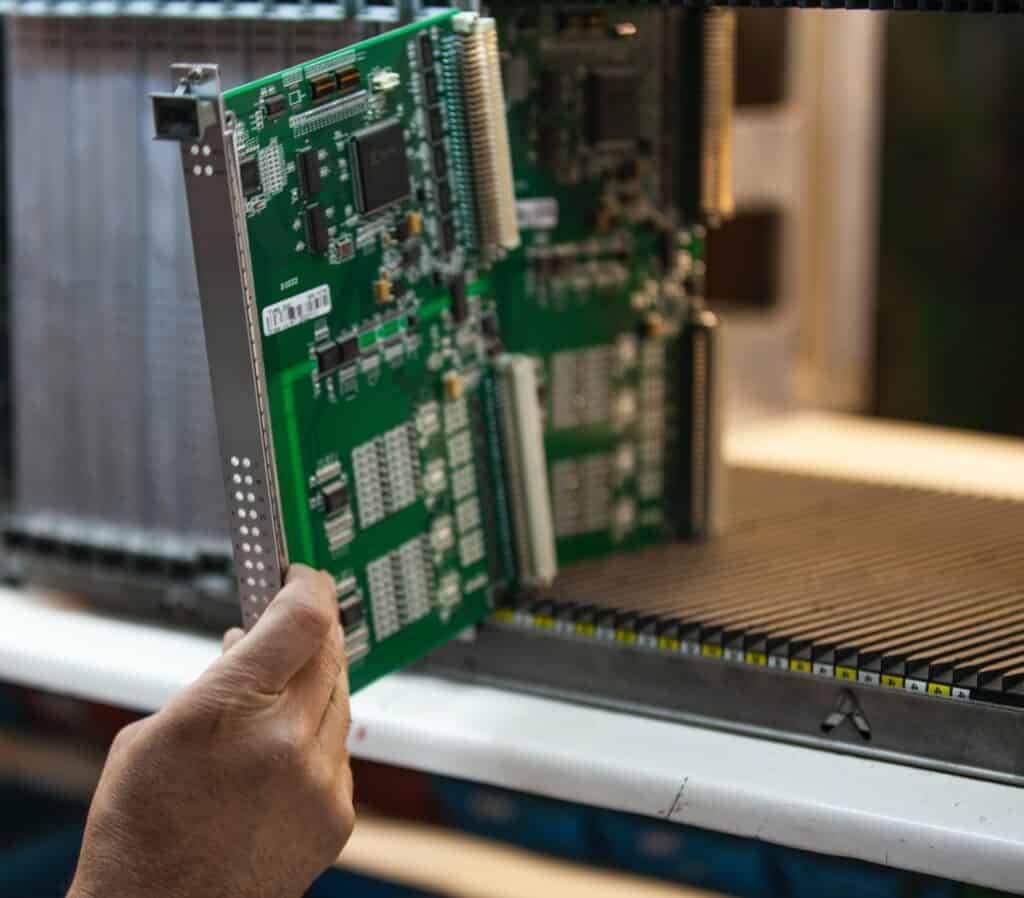
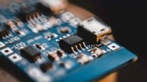
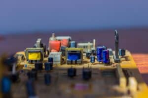
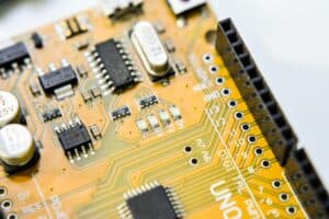
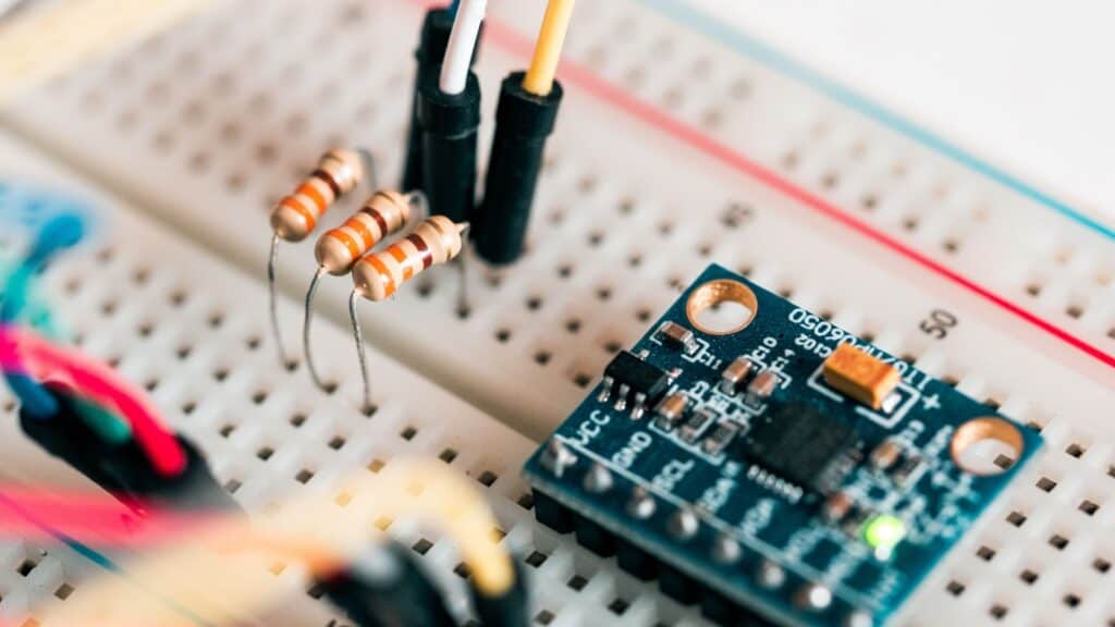
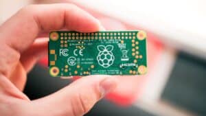
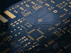
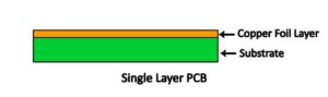
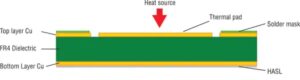
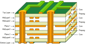
A PCB simply refers to a board made of fiberglass and laminate materials or a composite epoxy with conductive pathways. Printed circuit boards have a wide variety of both active and passive technological components—the components “talk” to each other to power the device they’re housed in. They come in many sizes to fit the needs of manufacturers and their customers.
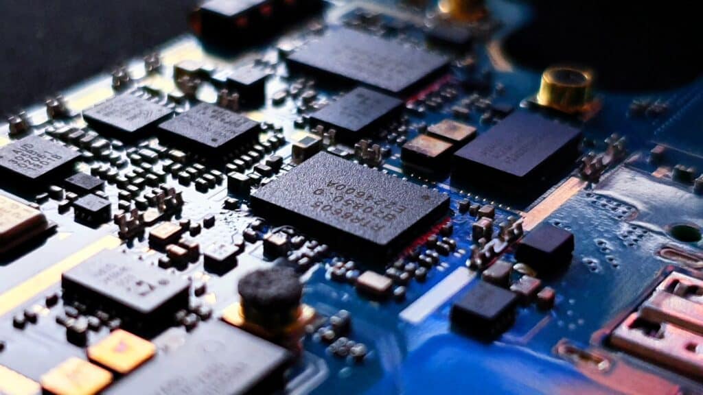
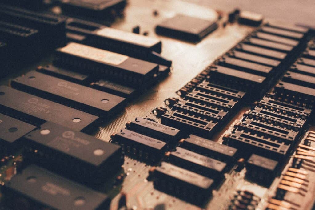
The pathways connect to various parts including transistors, resistors, and integrated circuits. Components are supported and connected electrically with special conductive pads or tracks. The electronic components are securely soldered onto a PCB to perform a specific function. Together, they make the heart of a well-operating piece of technology.
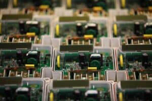
Manufacturers use PCBs because of the many advantages they offer. Some of these benefits are their compact size and lack of wires, ease of diagnostic and repair, time savings, compactness, cost savings, reliability, reduced noise, and short-circuit resistance due to tight connections.
How PCBs Are Used in Technology
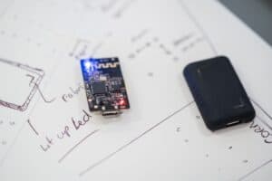
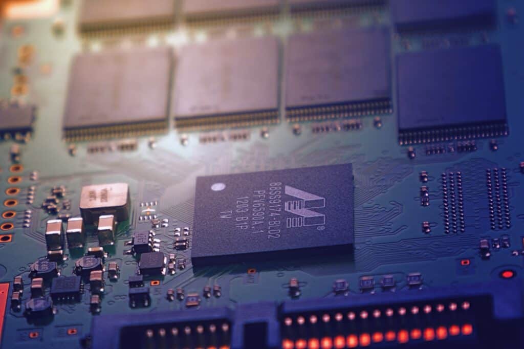
You may be surprised by the number of things you use every day that require a PCB to function. You probably own tens of devices that house a PCB. If you’re reading this on your smartphone or tablet, it’s relying on the quality of the PCB inside. Your smoke detector, TV remote, and electronic kitchen scale have circuit boards. And if there’s a problem with the circuit board, you can expect your electronics to operate poorly (if at all).
That’s because almost every device you can think of relies on the boards to make connections that would otherwise need wires and other bulky components. Even things like LEDs and industrial equipment need PCBs to function properly. Because of how common and critical PCBs are in our lives, it’s crucial that PCBs come from a reputable PCB manufacturer.
Quality control is one thing you can’t overlook if you want your electronics to live out their full expected lifespan and function effectively along the way.
What We Learned About PCBs
Put simply: there are countless things that wouldn’t work properly without PCBs. And with the cost and time savings manufacturers find after incorporating them into their processes, getting a PCB custom-made for a new product is a no-brainer. Printed circuit boards will only get more common, more efficient, and more reliable. As professionals and consumers in the industry get on board, it’s exciting to imagine the creative ways these beauties will be used in the future.
Why PCBs Are So Important in Today’s Technology Read More »