Blog

PCBs are so important

Why PCBs Are So Important in Today’s Technology

what are PCBs

What Are PCBs?

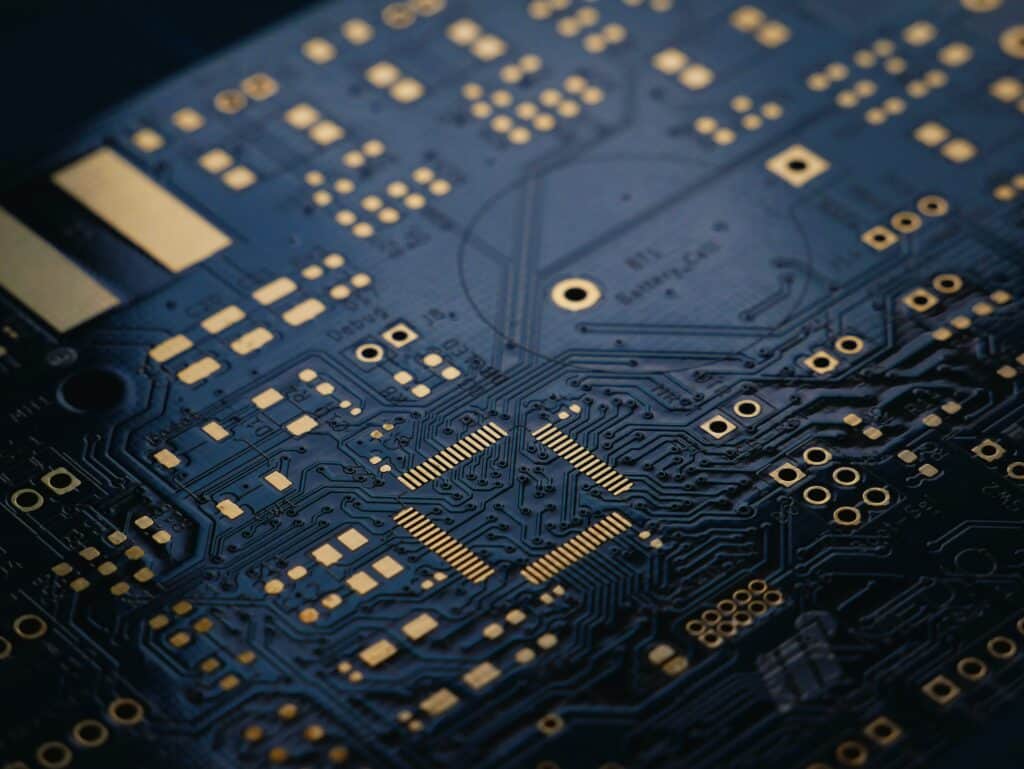
PCB simply refers to a board made of fiberglass and laminate materials or a composite epoxy with conductive pathways. Printed circuit boards have a wide variety of both active and passive technological components—the components “talk” to each other to power the device they’re housed in. They come in many sizes to fit the needs of manufacturers and their customers.

The pathways connect to various parts including transistors, resistors, and integrated circuits. Components are supported and connected electrically with special conductive pads or tracks. The electronic components are securely soldered onto a PCB to perform a specific function. Together, they make the heart of a well-operating piece of technology.

Manufacturers use PCBs because of the many advantages they offer. Some of these benefits are their compact size and lack of wires, ease of diagnostic and repair, time savings, compactness, cost savings, reliability, reduced noise, and short-circuit resistance due to tight connections.

How PCBs Are Used in Technology

You may be surprised by the number of things you use every day that require a PCB to function. You probably own tens of devices that house a PCB. If you’re reading this on your smartphone or tablet, it’s relying on the quality of the PCB inside. Your smoke detector, TV remote, and electronic kitchen scale have circuit boards. And if there’s a problem with the circuit board, you can expect your electronics to operate poorly (if at all).

That’s because almost every device you can think of relies on the boards to make connections that would otherwise need wires and other bulky components. Even things like LEDs and industrial equipment need PCBs to function properly. Because of how common and critical PCBs are in our lives, it’s crucial that PCBs come from a reputable PCB manufacturer.

Quality control is one thing you can’t overlook if you want your electronics to live out their full expected lifespan and function effectively along the way.

What We Learned About PCBs

Put simply: there are countless things that wouldn’t work properly without PCBs. And with the cost and time savings manufacturers find after incorporating them into their processes, getting a PCB custom-made for a new product is a no-brainer. Printed circuit boards will only get more common, more efficient, and more reliable. As professionals and consumers in the industry get on board, it’s exciting to imagine the creative ways these beauties will be used in the future.

Why PCBs Are So Important in Today’s Technology Read More »
Printed Circuit Board Assembly

Understanding the Printed Circuit Board Assembly (PCBA)

What is Printed Circuit Board Assembly? 

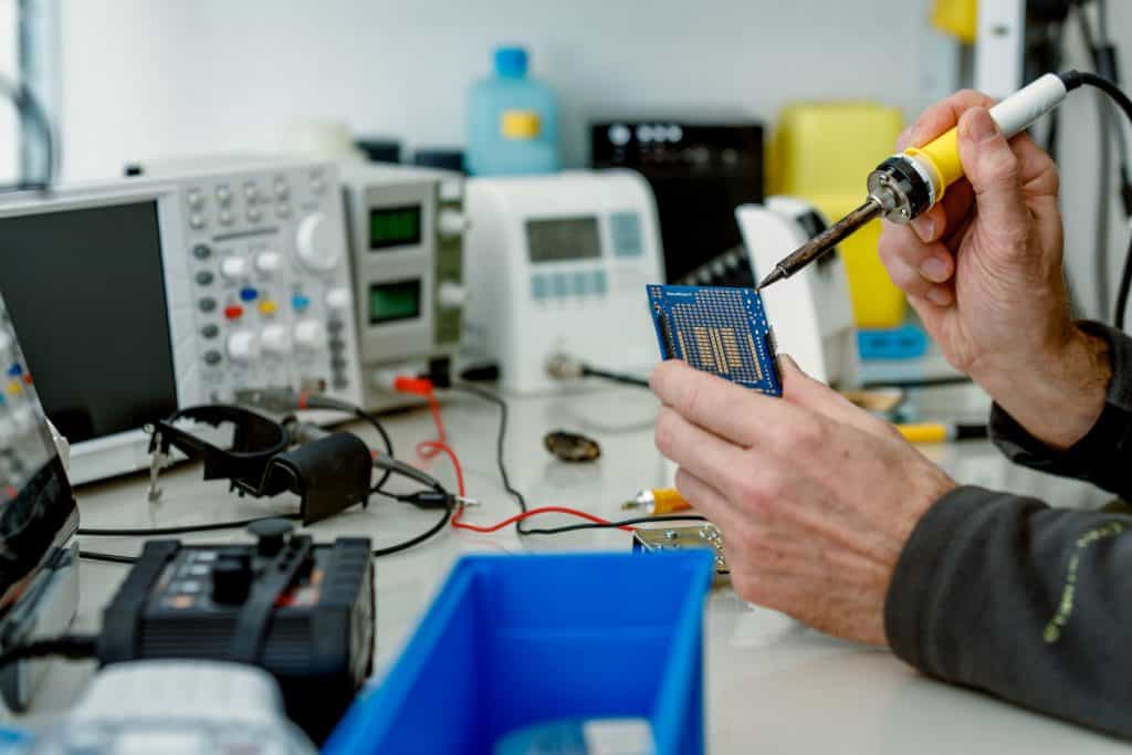
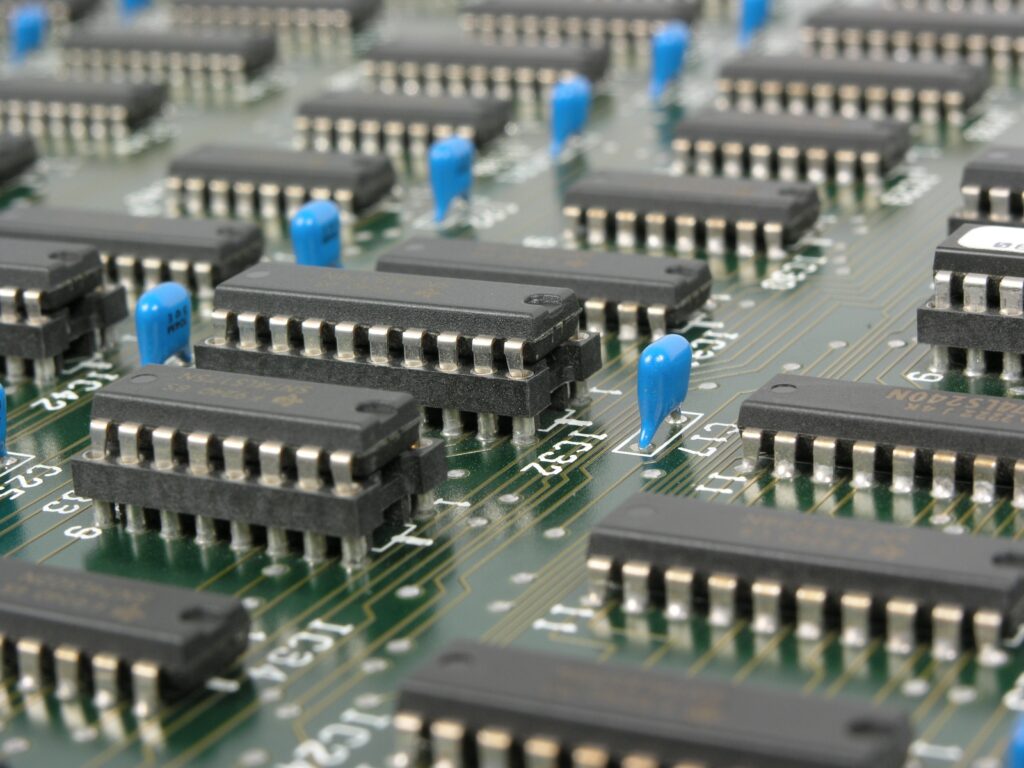
A circuit board prior to assembly of electronic components is known as PCB. Once electronic components are soldered, the board is called Printed Circuit Assembly (PCA) or Printed Circuit Board Assembly (PCBA) or PCB Assembly. Different Manual and Automatic PCB Assembly Tools are used in this process.

It has to be noted that the assembly of a circuit board is different from PCB Manufacturing Process. Manufacturing printed circuit boards involves several processes including PCB designing and creating PCB prototype. Once a PCB is ready, Active and Passive Electronic Components need to be soldered onto it before it can be used in any electronic equipment or gadget. This assembly of electronic components depends on Type of Printed Circuit Board, type of electronic components and purpose of the circuit board.

Printed Circuit Board Assembly with Thru-Hole Electronic Component

The first PCBs used through-hole technology, mounting electronic components by leads inserted through holes on one side of the board and soldered onto copper traces on the other side. Boards may be single-sided, with an unplanted component side, or more compact double-sided boards, with components soldered on both sides. Horizontal installation of through-hole parts with two axial leads (such as resistors, capacitors, and diodes) is done by bending the leads 90 degrees in the same direction, inserting the part in the board (often bending leads located on the back of the board in opposite directions to improve the part’s mechanical strength), soldering the leads, and trimming off the ends. Leads may be soldered either manually or by a wave soldering machine.

Through-hole manufacture adds to board cost by requiring many holes to be drilled accurately, and it limits the available routing area for signal traces on layers immediately below the top layer on multi-layer boards, since the holes must pass through all layers to the opposite side. Once surface-mounting came into use, small-sized SMD components were used where possible, with through-hole mounting only of components unsuitably large for surface-mounting due to power requirements or mechanical limitations, or subject to mechanical stress which might damage the PCB (e.g. by lifting the copper off the board surface).

Surface-Mount Technology for Printed Circuit Board Assembly

Surface-mount technology emerged in the 1960s, gained momentum in the early 1980s and became widely used by the mid-1990s. Components were mechanically redesigned to have small metal tabs or end caps that could be soldered directly onto the PCB surface, instead of wire leads to pass through holes. Components became much smaller and component placement on both sides of the board became more common than with through-hole mounting, allowing much smaller PCB assemblies with much higher circuit densities. Surface mounting lends itself well to a high degree of automation, reducing labor costs and greatly increasing production rates compared with through-hole circuit boards. Components can be supplied mounted on carrier tapes. Surface mount components can be about one-quarter to one-tenth of the size and weight of through-hole components, and passive components much cheaper. However, prices of semiconductor surface mount devices (SMDs) are determined more by the chip itself than the package, with little price advantage over larger packages, and some wire-ended components, such as 1N4148 small-signal switch diodes, are actually significantly cheaper than SMD equivalents.

Understanding the Printed Circuit Board Assembly (PCBA) Read More »

Why is PCB Prototyping So Important?

Why Is PCB Prototyping So Important? 

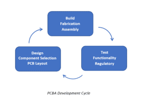
The essentialism of PCB prototyping is best understood by first clearly defining the circuit board development process, as shown below.

Prototyping boards

As illustrated above, developing circuit boards is typically cyclical and consists of numerous iterations. Each iteration is comprised of design, build, and test stages performed with the intent of improving the quality of the design. This technique of continually modifying the board until all errors have been corrected and the desired quality is achieved is known as PCB prototyping.

Advantages of Prototyping boards

When developing a PCB board, you need to make sure your design is free of error. You can test your designs through prototyping PCBs which is an extra step, but it will help save your time and money in the long run. By using prototype boards, you can also create several variations of the same circuit design to see which changes might work better than others. It can help to reduce the amount of rework that would need to be done in case your design has errors and resultantly give you a fast turnaround time.

Prototyping can help you locate areas you may need to make improvements to and locate potential issues in the design you may not have noticed only after manufactured. With thelp ofelp prototyping, you can even break down multiple PCB based components and individually test the different components to see that they operate just fine. This makes it easier to pinpoint the problems in more complex types of projects involving PCBs.

With the help of prototyping PCBs, you can get an idea of what your final product will look like.

Prototyping boards

The Role of Fabrication During PCB Prototyping

The building stage of development is where the physical embodiment of the design is constructed. During each iteration of the prototyping cycle, a new board is built or fabricated. Each new board, or set of boards, is then tested. During prototype, testing is primarily done to validate functionality and operation.

The fabrication process will yield a PCB or bare board, as shown above, where no elements are attached. Although, the locations for electronic component placement or footprints and corresponding pads are laid out. Subsequently, the components are connected to the board using through-hole soldering, surface mount technology (SMT), or a combination of the two to yield the final PCB assembly (PCBA), ready to be tested. Depending upon board complexity and your CM’s manufacturing, this process can take days or even weeks to yield a prototype.

To improve the overall speed of development, rapid PCB prototyping techniques have emerged that employ additive manufacturing. These additive manufacturing fabrication processes are capable of building prototypes in less than a day. And there are many options available for your PCB prototyping.

Prototyping boards

Why is PCB Prototyping So Important? Read More »

Understanding the PCB Fabrication and Assembly

PCB Fabrication and Assembly

Printed circuit board fabrication can be defined as a process of putting together the layers of the board along with particular surface patterns before making it fully usable for electronics manufacturing. In a way, it is an assembly method that can be done either by the manufacturing firms themselves or by outsourcing the service to third parties specializing in PCB fabrication.

The process of printed circuit board fabrication starts with a design or a diagram using client provided specifications and requirements. The Printed circuit board layout is an important part of the fabrication process. It involves a schematic design, which is created by the specialists after considering factors like: what the Printed circuit board is required to do, its functional attributes, and under what conditions would it be used. These details are provided by the customers or the clients to the PCB manufacturers who use the information for successful PCB fabrication.

PCB Fabrication and Assembly 

What is the PCB fabrication process? 

PCB fabrication is the process or procedure that transforms a circuit board design into a physical structure based upon the specifications provided in the design package. This physical manifestation is achieved through the following actions or techniques: Imaging desired layout on copper clad laminates. There have a few other terms and their interrelationships as below: –

  • PCB Development – can be defined as the process of taking a circuit board design from the design to the production. This typically includes three stages – design, manufacturing and testing. And for all but the simplest designs, this process is iterative with the objective of arriving at the highest quality design within the development time allotted.
  • PCB Manufacturing – can be defined as the construction o your board design. This is a two-step process that begins with board fabrication and ends with printed circuit board assembly (PCBA).
  • PCB Testing – sometimes referred to as bring up. is the third stage of PCB development; performed after manufacturing. Testing during development is done to evaluate the board’s ability to perform its intended operational functionality. During this stage, any error or areas where the design should be modified to improve performance are identified and another cycle is initiated to incorporate the design changes.
  • PCB Assembly – PCBA is the second step or stage of PCB manufacturing in which the board components are mounted to the bare board through a soldering process.

PCB Fabrication and Assembly 

Understanding the PCB Fabrication and Assembly Read More »

Overview of printed circuit boards (PCB)

PCBs are most commonly made out of fiberglass, composite, epoxy, or another composite material. Most PCBs for simple electronics are simple and composed of only a single layer. More sophisticated hardware such as computer graphics cards or motherboards can have multiple layers, sometimes up to twelve.

printed circuit boards (PCB)

Anatomy of a Printed Circuit Board (PCB)

As we all know what circuit boards look like: They’re thin, rigid, and usually rectangular, with components attached to one or both surfaces. The top and bottom are generally colored in dark blue or green. Lines running between the components have a slightly different color.  In addition to the top and bottom sides, modern circuit boards have internal planes called layers. Internal layers don’t have components but may contain metal lines the carry electricity to and from the components on the top and bottom. For example, the circuit board in the iPhone handset has 10 layers.

Layers are critically important in PCB design, so circuit board are commonly divided into three categories: single-sided, double-sided, or multilayer. This section discusses each of these categories and the manner in which the circuit boards are constructed.

Single-sided boards 

printed circuit boards (PCB)

The body of a single-sided board is made of a hard, nonconductive material, typically fiberglass epoxy-resin, or FR4. Some literature refers to a board’s material as substrate, the substrate thickness is given in thousandths of inches called mils (1 mil = 0.001 in). standard board thicknesses are 31 mils, 39 mils and 62 mils. A thin layer of metal is attached (usually glued or electrodeposited) to one side of the board, and will call this the top side. This metal is almost always copper, which is inexpensive and provides a low-resistance path for electricity.

Double-side boards 

printed circuit boards (PCB)

As the number of components on a board increases, so do the number of traces. In many instances, the full set of traces can’t be connected on a single plane without intersecting one another. To solve this problem, traces need a way to jump over other traces. This jumping is made possible by adding copper to the board’s bottom side. This bottom side may also support additional components. A board with copper on both sides is called a double-sided board.

Multilayer Boards 

printed circuit boards (PCB)

Double-sided boards enable more complex routing than single-sided boards, but sometimes two layers still aren’t enough. This occurs frequently when designing circuit whose components have hundreds of closely spaced leads. It’s also important for designs that require entire layers for ground or power supply. To resolve these issues, board designers create multilayer board designs. In essence, a multilayer board is a group of double-sided board sandwiched together using a material called prepreg. Similar to glue, prepreg is soft to begin with but hardens when heat and pressure are applied. A board’s arrangement of core and prepreg layers in a multilayer board is called its stack-up.

Overview of printed circuit boards (PCB) Read More »
The PCB Fabrication And Assembly

The PCB Fabrication And Assembly

PCB Services

Wingate Electronic Sdn Bhd was established in 2012. We provide one-stop services for PCB and PCBA. We can fabricate PCB up to 20 layers quick turn prototype and mass production high precision PCBs. ” The best quality, the lowest price, and the promptest delivery” is our principle. And our PCB assembly, we have automatic optical inspection (AOI) testers and can deal with all kinds of integrated circuits such as SMT, Through-hole components, and QFN. Our company can provide chip placement through-Hole components assembly and finished products fabrication.

The PCB Fabrication And Assembly

The PCB Fabrication and Assembly Services

Printed circuit board is a complex process that begins with a product concept and ends with a fully functional PCB assembly. The physical circuitry will be laid out in a PCB design after the net connectivity is captured. Finally, electronic components are ordered. We will solder the components onto the board, then the circuit board will be integrated into the full system. It will follow by assembly testing and verification.

The PCB Fabrication And Assembly

We need to take care of a lot of intricate details from the beginning to the end of PCB fabrication. One area in this process that doesn’t get the recognition it deserves is the fabrication of the bare board. The design of a PCB receives a lot of attention due to the complex software tools used in its creation. Manufacturing will get equally lauded in the satisfaction of completing the final product. But somewhere in the middle of this lies, the mysterious process of circuit board fabrication, often unknown outside of the design world.

The PCB Fabrication And Assembly

The PCB Fabrication And Assembly Read More »

Repair Industrial Electronic Devices Malaysia

Industrial Electronic Devices Repair In Malaysia

At Wingate Electronic Sdn Bhd, we can provide industrial electronic devices repair. Instead of throwing away the damaged circuit boards such as power supply, AC Inverter, DC inverter, touch screen monitor (HMI), servo amplifier, PLC, etc.

Do send them to us for a free evaluation and price quote for repair. “YOUR SMALL ACTION TODAY MIGHT TRANSLATE INTO A BIG SAVING TOMORROW.”

Repair Industrial Electronic Devices Malaysia

Repair Benefit

Nowadays, people rely on a truly large number of electronic devices. Many of them are fragile and prone to breaking. That can tempt people to simply go out and buy new ones. However, it is often better to repair them instead of replacing them. Fixing damaged electronics offers quite a few advantages, so it is something that everyone should consider when they suffer a malfunction.

Repair Industrial Electronic Devices Malaysia

Save Money 

Nowadays New electronics are expensive, especially when they are the latest and greatest model to hit the market. Most people struggle to find the money to replace a damaged device without warning, and even those who can afford it often find that it causes some financial strain. Repairing damaged electronics is normally cheaper than replacing them, especially for larger or more complex devices. It is still important to check the prices before making a choice, but it is generally safe to assume that repairs are the financially responsible option.

Repair Industrial Electronic Devices Malaysia

Save Time

Most people spend a lot of time picking out a new device. They compare models, look for sales, and read reviews. That is vital to make a good choice, and we could actually spend on doing other tasks. Sending a device out for repairs is faster and ideal for people who have busy lives. It is also beneficial to those who cannot spare the time to do the research for a new device.

Repair Industrial Electronic Devices Malaysia

No Learning Curve

It will take a huge amount of time for us to get to use a new device. Especially if that device is a major upgrade over an old one. Most people can get used to any new design with time and effort, but they suffer a major loss to productivity while they adapt. It can also be a deeply frustrating experience. That makes it a problem for both businesses that need their employees to perform at their best and for private individuals who want a device that just works. Sticking to older electronics eliminates that learning curve, which makes it the most convenient option for the vast majority of people.

Know Outcome

Even people who do their research sometimes find that new devices do not meet their expectations. That leads to stress, disappointment, and wasted money. A repaired device is a known outcome, so the owner will rarely be surprised by the result. They can simply go back to use the device that they have gotten used to using.

Industrial Electronic Devices Repair In Malaysia Read More »

2018 AI And Robotic Predictions

2018 AI And Robotic Predictions

“In the information industry and at Thomson Reuters, AI and machine learning are already driving innovation and transformation. They are embedded in how we sift through large volumes of data and content and how we enhance, organize, connect, and deliver content and information. They are the engines underlying many of our products and services.” Dr. Khalid Al-Kofahi -Vice President, R&D and Head of the Center for AI and Cognitive Computing

When things go digital, they start following a new set of rules.

The rules of the physical world are either not applicable or are severely diminished. Things move from sparsity to abundance, where consumption does not lead to depletion. On the contrary, the more an object is consumed, the more valuable it becomes. Cost of production and distribution is no longer critical, and the concept of inventory is no longer applicable.

When things go digital, they also move from linear to exponential – a world in which new technologies and new players can enter and dominate an industry in just a few years.

Consider that each year more people take online courses offered by Harvard than the number of students who attended Harvard in its 380-year history. Each year, three times more people use online dispute resolutions to resolve disputes on eBay than lawsuits filed in the United States. Each day, five billion videos are watched on YouTube. For context, the first YouTube video was uploaded in 2005. I was talking to a gentleman at Facebook a few weeks ago who said, “I joined Facebook three years ago and 70 percent of the company started after me.” Talk about hyper-growth businesses!

This is the environment that we operate in: Not only must we adapt, but we must help our customers adapt as well.

In the information industry and at Thomson Reuters, AI and machine learning (ML) are already driving innovation and transformation. They are embedded in how we sift through large volumes of data and content, and how we enhance, organize, connect, and deliver content and information. They are the engines underlying many of our products and services.

In the long term, our objective is to build personal digital assistants for knowledge workers. An assistant is an application that:

  • Interacts naturally with you
  • Is both responsive and proactive (without being intrusive)
  • The collection of all of your professional experiences
  • Available with a few words and a click
  • Learns from you as well as others (via their digital assistants)

Its purpose is not to replace you, but to augment you, to scale you, and to help you focus on more interesting tasks.

It will probably take a decade or two to build some of these digital assistants – but the near term is also full of interesting opportunities to transform, through simplification, automation, and machine assistance.

Research and Discovery

Research, discovery, and investigation represent a significant portion of what knowledge workers do. These are complex and time-consuming tasks, making them easy contenders for simplification, automation, and machine assistance.

Information Overload

Our world is connected and information-rich. The cycle of information creation is continuous and instant, and staying informed can be a daunting task. One of our primary objectives is to pivot away from customers finding information to the information finding the customer.

Risk and Compliance

This theme focuses on helping our customers comply with relevant laws and regulations, discover risks that could disrupt their businesses, and respond appropriately when things happen.

Making Sense

Knowledge work requires making sense of data in order to make time-sensitive and business-critical decisions. Whether it is a single document or collection of documents, an event, a work product, or an “abnormal” pattern, making sense is hard and time-consuming. AI can help.

This is just a selection of key focus areas based on analysis and discussions with our customers and business partners. The predictions in this report dive deeper into each of these opportunities. What is clear is that AI and machine learning are already here and their potential to assist knowledge workers is being realized.

2018 AI And Robotic Predictions Read More »

industry 4.0

Industry 4.0

“Industry 4.0” refers to the fourth industrial revolution. After mechanization (Industry 1.0), mass production (Industry 2.0), and automation (Industry 3.0), now the “internet of things and services’ is becoming an integral part of manufacturing. Industry 4.0 technologies have the potential to create extraordinary growth opportunities and competitive advantages for Germany as a business location. Experts forecast that businesses will be able to increase their productivity by about 30 percent using Industry 4.0’’ – BDI The Voice of German Industry

“INDUSTRIE 4.0 connects embedded system production technologies and smart production processes to pave the way to a new technological age which will radically transform industry and production value chains and business models.’’ – Germany Trade and Invest

Embracing Industry 4.0 – and Rediscovering Growth

“What is existing manufacturing and large technological innovations coming together to create the next big manufacturing reinvention? Bingo. This is the fourth manufacturing revolution, and it’s happening right now.” – OLIVIER SCALABRE Senior Partner & Managing Director Paris

The rise of new digital industrial technology, known as Industry 4.0, is a transformation that makes it possible to gather and analyze data across machines, enabling faster, more flexible, and more efficient processes to produce higher-quality goods at reduced costs. This manufacturing revolution will increase productivity, shift economics, foster industrial growth, and modify the profile of the workforce—ultimately changing the competitiveness of companies and regions.

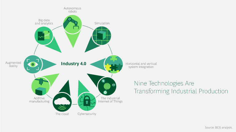
Nine Technologies Transforming Industrial Production

Advanced digital technology is already used in manufacturing, but Industry 4.0 will transform production. It will lead to greater efficiencies and change traditional production relationships among suppliers, producers, and customers—as well as between humans and machines. Nine technology trends form the building blocks of Industry 4.0.

adopting industry 4.0

Adopting Industry 4.0

Companies face formidable challenges in the adoption of these new technologies. To build and sustain a lead in the race to full implementation, they need to broaden and deepen their practical knowledge about digital technologies and the related use cases—and then develop and implement tailored digital manufacturing strategies.

BCG’s approach to Industry 4.0—along with the firm’s state-of-the-art model factories, or Innovation Centers for Operations—provides companies with the support they need to master the challenges of implementation.

Industry 4.0 Read More »

Product Enquiry

Scroll to Top