Why Is PCB Prototyping So Important?
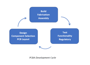
The essentialism of PCB prototyping is best understood by first clearly defining the circuit board development process, as shown below.

As illustrated above, developing circuit boards is typically cyclical and consists of numerous iterations. Each iteration is comprised of design, build, and test stages performed with the intent of improving the quality of the design. This technique of continually modifying the board until all errors have been corrected and the desired quality is achieved is known as PCB prototyping.
Advantages of Prototyping boards
When developing a PCB board, you need to make sure your design is free of error. You can test your designs through prototyping PCBs which is an extra step, but it will help save your time and money in the long run. By using prototype boards, you can also create several variations of the same circuit design to see which changes might work better than others. It can help to reduce the amount of rework that would need to be done in case your design has errors and resultantly give you a fast turnaround time.
Prototyping can help you locate areas you may need to make improvements to and locate potential issues in the design you may not have noticed only after manufactured. With thelp ofelp prototyping, you can even break down multiple PCB based components and individually test the different components to see that they operate just fine. This makes it easier to pinpoint the problems in more complex types of projects involving PCBs.
With the help of prototyping PCBs, you can get an idea of what your final product will look like.

The Role of Fabrication During PCB Prototyping
The building stage of development is where the physical embodiment of the design is constructed. During each iteration of the prototyping cycle, a new board is built or fabricated. Each new board, or set of boards, is then tested. During prototype, testing is primarily done to validate functionality and operation.
The fabrication process will yield a PCB or bare board, as shown above, where no elements are attached. Although, the locations for electronic component placement or footprints and corresponding pads are laid out. Subsequently, the components are connected to the board using through-hole soldering, surface mount technology (SMT), or a combination of the two to yield the final PCB assembly (PCBA), ready to be tested. Depending upon board complexity and your CM’s manufacturing, this process can take days or even weeks to yield a prototype.
To improve the overall speed of development, rapid PCB prototyping techniques have emerged that employ additive manufacturing. These additive manufacturing fabrication processes are capable of building prototypes in less than a day. And there are many options available for your PCB prototyping.


