pcb fabrication

Why do we need Multilayer PCB?

The Advantages of Multilayer PCB

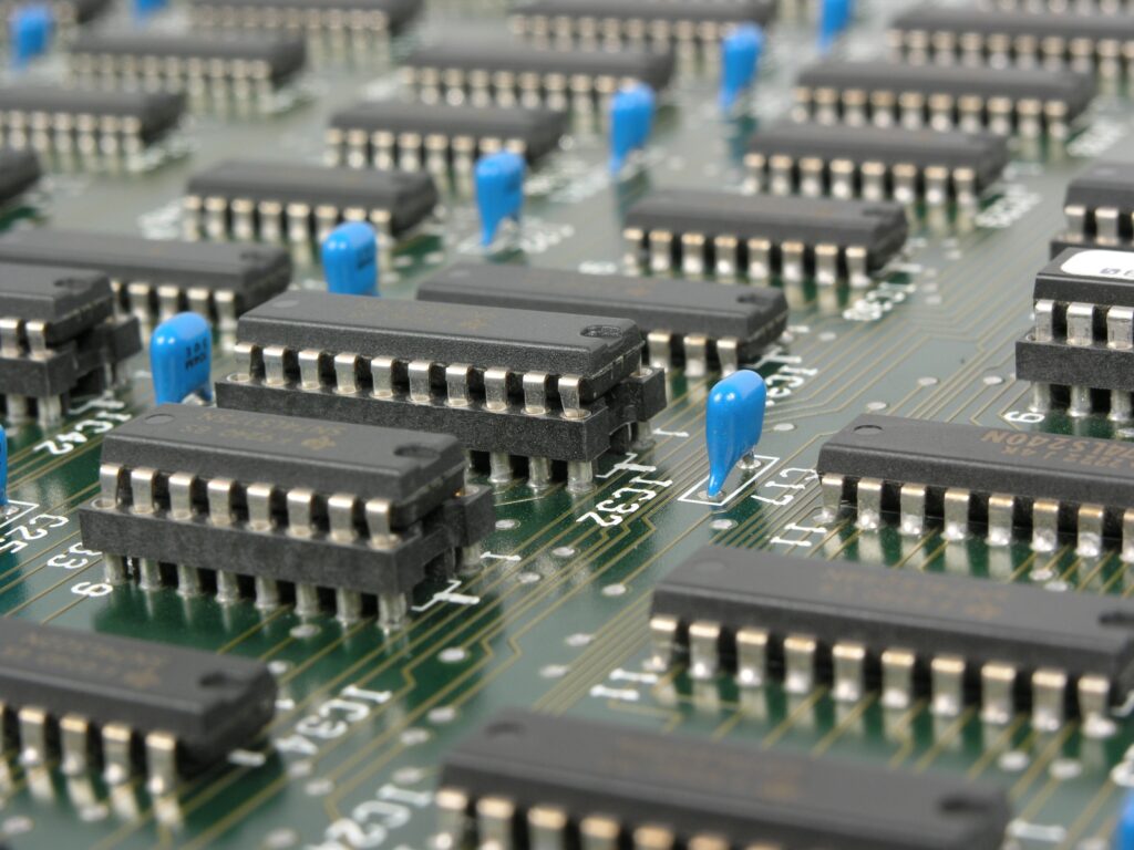
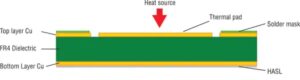
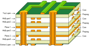
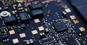
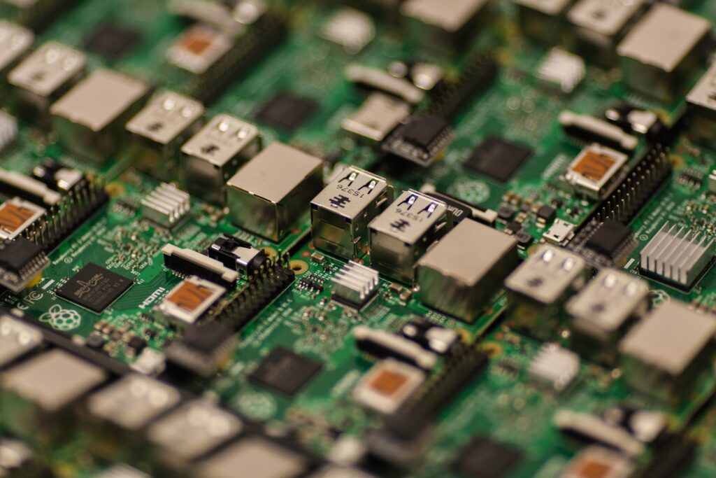
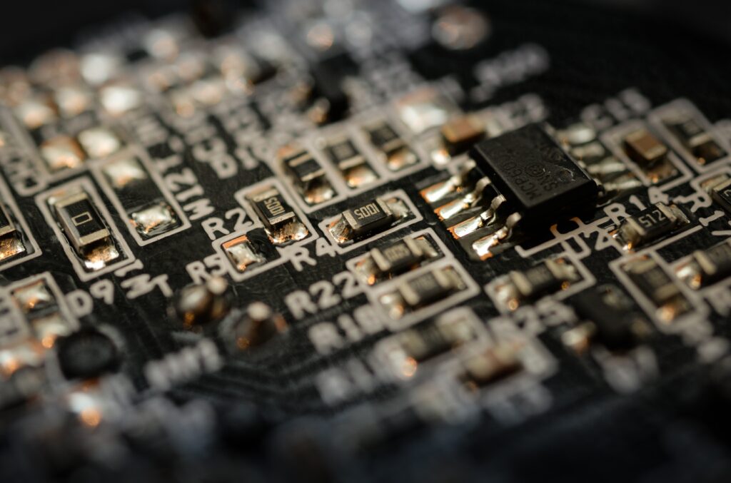
Having more layers means the board is thicker and, therefore, more durable than single-sided PCBs. This is another reason adding functionality through additional layers is preferable to increase the dimensions of a single layer. Printed circuit boards have ubiquitous presence today, what with them being the core of most electronic items. With the growing complexity of devices, Printed circuit boards are therefore increasingly becoming more complex. From flexible to odd shaped ones, there is a range of PCBS out there. While electronic devices with limited functions can do with single layer PCBs, there is an exponential growth in multi layered PCBs. By definition, multilayered PCB are made up of layers of double-sided circuit boards with heat protective insulation between them. The electrical connections between the layers happen through various kinds of vias resulting in complex multilayered PCBs. With complexity in applications, PCBs today can range anywhere from four to twelve layers.

  • Size: Multilayer PCB have an added advantage on account of their small size as they lend themselves well.
  • Lightweight: Small PCBs also come with reduced weight. This is particularly true also because single and double layered PCBs need a number of connectors that add to the weight and hence restrict mobility.
  • Reliability: Typically multilayered PCBs are high on reliability as well as of high quality.
  • Durability: Multilayer PCBs also come with high durability as they are able to withstand the heat and pressure that is applied on them.
  • Flexibility: For assemblies that use flexible construction techniques, a flexible multilayered PCB can be helpful particularly in applications that require some amount of bending.
  • Powerful: Multilayer PCBs typically are high density and have greater capacity as well as speed.
  • Single Connection Point: With single connection points, multilayered PCBs are beneficial for gadgets where size and weight are constraints.

On account of all these advantages, multilayer PCBs are the preferred option especially as greater functionality and reduced size increasingly become the norm.

All of this is not to say that multilayered PCB Fabrication does not have any disadvantages. Largely, compared to single layered PCBs, multilayered ones come with added cost as well as increased design time. Multi layered PCBs also necessitate that there be skilled designers who have a wide experience and hence can overcome issues related to crosstalk and impedance. In efficient design it can directly impact board functioning.  Also, multilayer boards require increased production time and hence a lower turnover rate.

However, it is their improved functionality that more than covers for the many disadvantages associated with multi layered boards. As far as their increased costs go, with the advancement of technology, the costs are only slated to decrease.

However, even while using multi layered PCBs it is important to ensure that as far as possible you go with an even number of layers as opposed to PCBs with odd number of layers. This is on account of many factors including but not limited to the cost efficiency:

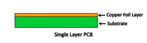
Single layer PCBs are cost ineffective

The cost ineffectiveness of odd number of layers stems from the fact that the process of creating an odd layered PCB begins with creating an even layered PCB and then etching away the unwanted layer. As the process suggests, this leads to a lot of wastage which in turn lead to cost inefficiencies.

Warping

Other than the cost aspect, etching also results in warping of the layer. With one side having copper and the other side not having it, there are different cooling rates, thereby creating stress on the PCB.

Risk of over & under plating

What the etching also does is that it leaves the two sides (one with copper and one without), with different weights, thereby adding to the risk of under or over plating.

On account of all the above reasons, it isn’t advisable to have single layers unless there is a specific, compelling reason to do so.

Why do we need Multilayer PCB? Read More »

To Design a good PCB stack-up

The rules and standard for designing a good PCB stack-up

The rules and standards for designing a good stack-up are hundreds. Let’s just see a few:

  • Ground plane boards are better because they allow signal routing in a microstrip or strip-line configuration. It also significantly reduces the ground impedance and, therefore, the ground noise;
  • High speed signals should be “routed” on intermediate layers located between the various levels. In this way, ground planes can act as a shield and contain the radiation coming from the tracks at high speed;
  • The signal layers should be very close to each other, even in adjacent planes.
  • A signal layer must always be adjacent to a plane;
  • Multiple ground planes are very advantageous, since they lower the board’s ground impedance and reduce radiation in a common way;
  • The power and mass planes must be rigorously coupled together;

To achieve all these objectives, it is necessary to operate with a minimum of eight layers. Moreover:

  • From a mechanical point of view, it is advisable to implement a cross section to avoid deformations;
  • Configurations should be symmetric. For example, on an eight-layer PCB, if level 2 is a plane, level 7 should also be a plane;
  • If the signal levels are next to the levels of the plane (ground or power) the return current can flow on an adjacent plane reducing the inductance of the return path to a minimum;
  • To further improve noise and EMI performance, insulation between a signal layer and its adjacent plane can be made even thinner;
  • An important consideration to be made is the thickness of each signal layer. There are standard thicknesses together with the properties of different types of printed circuit material. When selecting the materials, it is advisable to consider their electrical, mechanical and thermal properties;
  • Use excellent software to help you design your stack-up. All this should be done in order to choose the correct materials from the library and perform impedance calculations based on the materials and their dimensions.

Careful PCB design is necessary

Proto-Electronics’ mission is to help you in this crucial prototyping phase by cutting your lead times. Online quotes in 10 minutes and delivery lead times starting from 5 working days will give you more peace of mind to work.

To Design a good PCB stack-up Read More »

Multilayer PCB stackup

Multilayer PCB Layer Stack-up

PCB Layer Stack-Up

The single core is good for up to 4 layers of PCB, but for more layers like for 6 layers there should be 2 cores and for 8 layers there should be 3 cores. The layers are always taken in even numbers for the purpose of uniformity in layer stack.  

The multi-layer PCB is the combination of two or more single- or double-sided PCBs hence a strong mutual connection is in between. The increasing complexity of multilayer PCB gives rise to some typical issues that are noise, signal interference, cross talk, stray capacitances and impedance mismatches. These issues need to be professionally handled otherwise the overall PCB performance and reliability can greatly shatter.

A properly designed layer stack up can help reduce circuit’s vulnerability to Electromagnetic Interference (EMI) and external noises that can distort high speed signals. A good layer stack up also helps to avoid cross talks, improves signal integrity and impedance matching can reduce power losses. The perfect layer stack can also reduce the cost of manufacturing multilayer PCB.

The multilayer stack up will enable you to place more circuitry in the limited space while diverting your routing to internal signal layers by means of blind and buried via. Separate ground GND and power PWR planes are used which are also copper layers.

The layer stack up should be symmetrical and the minimum clearance between traces, layers spacing, and the thickness of core should be carefully taken. The thickness of the core can be from 0.1mm to 0.3mm.

The base substrate core material FR-4 is pre-impregnated with epoxy resin system. The pre-preg is used as the adhesive to form the laminated stack of these multiple layers. This is done by lamination machine that works under high temperature and pressure.

What is Multilayer PCB Stack-up? 

A stack-up is the arrangement of layers of copper and insulators that make up a PCB before designing the final layout of the board. Managing a good stack-up is not exactly easy and companies that make multilayer printed circuits such as Proto-Electronics, a platform dedicated to the rapid prototyping of SMT printed circuits and cross-section components, for professionals, must be at the forefront.

Having multiple layers increases the board’s ability to distribute energy, reduces cross-interference, eliminates electromagnetic interference and supports high-speed signals. While a stack-up level allows you to get multiple electronic circuits on a single board through the various layers of PCB board, the structure of the PCB stack-up design provides many other advantages:

  1. A stack of PCB layers can help minimize the circuit vulnerability to external noise, as well as minimize radiation and decrease impedance and crosstalk problems on high-speed systems;
  2. A good PCB stacking can also contribute to efficient and low-cost final production;
  3. A correct stack of PCB layers can improve the electromagnetic compatibility of the project.

With a single-layer or double-layer PCB the board thickness is rarely considered. However, with the advent of multilayer PCBs, the pile of materials is starting to become more and more critical and the final cost is the factor that affects the entire project. The simplest stack-ups can include 4-layer PCBs, up to the more complex ones that require professional sequential lamination. The higher the number of layers, the more the designer is free to unravel his circuit, with less chance of stumbling into “impossible” solutions. The PCB overlapping operations consist in the arrangement of the copper layers and the insulating layers that make up a circuit. The back-up you choose certainly plays an important role in the performance of the board in several ways.

For example, good layering can reduce the impedance of the board and limit radiation and crosstalk. It also has a major impact on the EMC performance of a product. On the other hand, poor stack-up design can significantly increase circuit radiation and noise. There are four important factors to consider when dealing with board stack-up:

  1. Number of Layers
  2. The number and types of plans used (power plans and ground plans);
  3. Sorting and sequence of levels;
  4. Spacing between levels.

Usually, not much consideration is given to these factors, except for those affecting the number of layers. Often the fourth factor is not even known to the PCB designer. When deciding on the number of layers, you need to consider the following:

  1. The number of signals to be routed and their cost;
  2. Operating frequency;
  3. Whether the product will meet Class A or Class B emission requirements;
  4. Whether the PCB will be in a shielded container or not;
  5. Whether the design team is competent in EMC rules and regulations.

All factors are important and critical and should be considered equally. Multilayer boards that use mass and power plane provide a significant reduction in radiated emissions. A rule of thumb, which is often used, is that a four-layer board will produce 15 dB less radiation than a two-layer board, all other factors being equal.

Multilayer PCB Layer Stack-up Read More »

Printed Circuit Board Assembly

Understanding the Printed Circuit Board Assembly (PCBA)

What is Printed Circuit Board Assembly? 

A circuit board prior to assembly of electronic components is known as PCB. Once electronic components are soldered, the board is called Printed Circuit Assembly (PCA) or Printed Circuit Board Assembly (PCBA) or PCB Assembly. Different Manual and Automatic PCB Assembly Tools are used in this process.

It has to be noted that the assembly of a circuit board is different from PCB Manufacturing Process. Manufacturing printed circuit boards involves several processes including PCB designing and creating PCB prototype. Once a PCB is ready, Active and Passive Electronic Components need to be soldered onto it before it can be used in any electronic equipment or gadget. This assembly of electronic components depends on Type of Printed Circuit Board, type of electronic components and purpose of the circuit board.

Printed Circuit Board Assembly with Thru-Hole Electronic Component

The first PCBs used through-hole technology, mounting electronic components by leads inserted through holes on one side of the board and soldered onto copper traces on the other side. Boards may be single-sided, with an unplanted component side, or more compact double-sided boards, with components soldered on both sides. Horizontal installation of through-hole parts with two axial leads (such as resistors, capacitors, and diodes) is done by bending the leads 90 degrees in the same direction, inserting the part in the board (often bending leads located on the back of the board in opposite directions to improve the part’s mechanical strength), soldering the leads, and trimming off the ends. Leads may be soldered either manually or by a wave soldering machine.

Through-hole manufacture adds to board cost by requiring many holes to be drilled accurately, and it limits the available routing area for signal traces on layers immediately below the top layer on multi-layer boards, since the holes must pass through all layers to the opposite side. Once surface-mounting came into use, small-sized SMD components were used where possible, with through-hole mounting only of components unsuitably large for surface-mounting due to power requirements or mechanical limitations, or subject to mechanical stress which might damage the PCB (e.g. by lifting the copper off the board surface).

Surface-Mount Technology for Printed Circuit Board Assembly

Surface-mount technology emerged in the 1960s, gained momentum in the early 1980s and became widely used by the mid-1990s. Components were mechanically redesigned to have small metal tabs or end caps that could be soldered directly onto the PCB surface, instead of wire leads to pass through holes. Components became much smaller and component placement on both sides of the board became more common than with through-hole mounting, allowing much smaller PCB assemblies with much higher circuit densities. Surface mounting lends itself well to a high degree of automation, reducing labor costs and greatly increasing production rates compared with through-hole circuit boards. Components can be supplied mounted on carrier tapes. Surface mount components can be about one-quarter to one-tenth of the size and weight of through-hole components, and passive components much cheaper. However, prices of semiconductor surface mount devices (SMDs) are determined more by the chip itself than the package, with little price advantage over larger packages, and some wire-ended components, such as 1N4148 small-signal switch diodes, are actually significantly cheaper than SMD equivalents.

Understanding the Printed Circuit Board Assembly (PCBA) Read More »

Why is PCB Prototyping So Important?

Why Is PCB Prototyping So Important? 

The essentialism of PCB prototyping is best understood by first clearly defining the circuit board development process, as shown below.

Prototyping boards

As illustrated above, developing circuit boards is typically cyclical and consists of numerous iterations. Each iteration is comprised of design, build, and test stages performed with the intent of improving the quality of the design. This technique of continually modifying the board until all errors have been corrected and the desired quality is achieved is known as PCB prototyping.

Advantages of Prototyping boards

When developing a PCB board, you need to make sure your design is free of error. You can test your designs through prototyping PCBs which is an extra step, but it will help save your time and money in the long run. By using prototype boards, you can also create several variations of the same circuit design to see which changes might work better than others. It can help to reduce the amount of rework that would need to be done in case your design has errors and resultantly give you a fast turnaround time.

Prototyping can help you locate areas you may need to make improvements to and locate potential issues in the design you may not have noticed only after manufactured. With thelp ofelp prototyping, you can even break down multiple PCB based components and individually test the different components to see that they operate just fine. This makes it easier to pinpoint the problems in more complex types of projects involving PCBs.

With the help of prototyping PCBs, you can get an idea of what your final product will look like.

Prototyping boards

The Role of Fabrication During PCB Prototyping

The building stage of development is where the physical embodiment of the design is constructed. During each iteration of the prototyping cycle, a new board is built or fabricated. Each new board, or set of boards, is then tested. During prototype, testing is primarily done to validate functionality and operation.

The fabrication process will yield a PCB or bare board, as shown above, where no elements are attached. Although, the locations for electronic component placement or footprints and corresponding pads are laid out. Subsequently, the components are connected to the board using through-hole soldering, surface mount technology (SMT), or a combination of the two to yield the final PCB assembly (PCBA), ready to be tested. Depending upon board complexity and your CM’s manufacturing, this process can take days or even weeks to yield a prototype.

To improve the overall speed of development, rapid PCB prototyping techniques have emerged that employ additive manufacturing. These additive manufacturing fabrication processes are capable of building prototypes in less than a day. And there are many options available for your PCB prototyping.

Prototyping boards

Why is PCB Prototyping So Important? Read More »

Understanding the PCB Fabrication and Assembly

PCB Fabrication and Assembly

Printed circuit board fabrication can be defined as a process of putting together the layers of the board along with particular surface patterns before making it fully usable for electronics manufacturing. In a way, it is an assembly method that can be done either by the manufacturing firms themselves or by outsourcing the service to third parties specializing in PCB fabrication.

The process of printed circuit board fabrication starts with a design or a diagram using client provided specifications and requirements. The Printed circuit board layout is an important part of the fabrication process. It involves a schematic design, which is created by the specialists after considering factors like: what the Printed circuit board is required to do, its functional attributes, and under what conditions would it be used. These details are provided by the customers or the clients to the PCB manufacturers who use the information for successful PCB fabrication.

PCB Fabrication and Assembly 

What is the PCB fabrication process? 

PCB fabrication is the process or procedure that transforms a circuit board design into a physical structure based upon the specifications provided in the design package. This physical manifestation is achieved through the following actions or techniques: Imaging desired layout on copper clad laminates. There have a few other terms and their interrelationships as below: –

  • PCB Development – can be defined as the process of taking a circuit board design from the design to the production. This typically includes three stages – design, manufacturing and testing. And for all but the simplest designs, this process is iterative with the objective of arriving at the highest quality design within the development time allotted.
  • PCB Manufacturing – can be defined as the construction o your board design. This is a two-step process that begins with board fabrication and ends with printed circuit board assembly (PCBA).
  • PCB Testing – sometimes referred to as bring up. is the third stage of PCB development; performed after manufacturing. Testing during development is done to evaluate the board’s ability to perform its intended operational functionality. During this stage, any error or areas where the design should be modified to improve performance are identified and another cycle is initiated to incorporate the design changes.
  • PCB Assembly – PCBA is the second step or stage of PCB manufacturing in which the board components are mounted to the bare board through a soldering process.

PCB Fabrication and Assembly 

Understanding the PCB Fabrication and Assembly Read More »

Overview of printed circuit boards (PCB)

PCBs are most commonly made out of fiberglass, composite, epoxy, or another composite material. Most PCBs for simple electronics are simple and composed of only a single layer. More sophisticated hardware such as computer graphics cards or motherboards can have multiple layers, sometimes up to twelve.

printed circuit boards (PCB)

Anatomy of a Printed Circuit Board (PCB)

As we all know what circuit boards look like: They’re thin, rigid, and usually rectangular, with components attached to one or both surfaces. The top and bottom are generally colored in dark blue or green. Lines running between the components have a slightly different color.  In addition to the top and bottom sides, modern circuit boards have internal planes called layers. Internal layers don’t have components but may contain metal lines the carry electricity to and from the components on the top and bottom. For example, the circuit board in the iPhone handset has 10 layers.

Layers are critically important in PCB design, so circuit board are commonly divided into three categories: single-sided, double-sided, or multilayer. This section discusses each of these categories and the manner in which the circuit boards are constructed.

Single-sided boards 

printed circuit boards (PCB)

The body of a single-sided board is made of a hard, nonconductive material, typically fiberglass epoxy-resin, or FR4. Some literature refers to a board’s material as substrate, the substrate thickness is given in thousandths of inches called mils (1 mil = 0.001 in). standard board thicknesses are 31 mils, 39 mils and 62 mils. A thin layer of metal is attached (usually glued or electrodeposited) to one side of the board, and will call this the top side. This metal is almost always copper, which is inexpensive and provides a low-resistance path for electricity.

Double-side boards 

printed circuit boards (PCB)

As the number of components on a board increases, so do the number of traces. In many instances, the full set of traces can’t be connected on a single plane without intersecting one another. To solve this problem, traces need a way to jump over other traces. This jumping is made possible by adding copper to the board’s bottom side. This bottom side may also support additional components. A board with copper on both sides is called a double-sided board.

Multilayer Boards 

printed circuit boards (PCB)

Double-sided boards enable more complex routing than single-sided boards, but sometimes two layers still aren’t enough. This occurs frequently when designing circuit whose components have hundreds of closely spaced leads. It’s also important for designs that require entire layers for ground or power supply. To resolve these issues, board designers create multilayer board designs. In essence, a multilayer board is a group of double-sided board sandwiched together using a material called prepreg. Similar to glue, prepreg is soft to begin with but hardens when heat and pressure are applied. A board’s arrangement of core and prepreg layers in a multilayer board is called its stack-up.

Overview of printed circuit boards (PCB) Read More »

The PCB Fabrication And Assembly

The PCB Fabrication And Assembly

PCB Services

Wingate Electronic Sdn Bhd was established in 2012. We provide one-stop services for PCB and PCBA. We can fabricate PCB up to 20 layers quick turn prototype and mass production high precision PCBs. ” The best quality, the lowest price, and the promptest delivery” is our principle. And our PCB assembly, we have automatic optical inspection (AOI) testers and can deal with all kinds of integrated circuits such as SMT, Through-hole components, and QFN. Our company can provide chip placement through-Hole components assembly and finished products fabrication.

The PCB Fabrication And Assembly

The PCB Fabrication and Assembly Services

Printed circuit board is a complex process that begins with a product concept and ends with a fully functional PCB assembly. The physical circuitry will be laid out in a PCB design after the net connectivity is captured. Finally, electronic components are ordered. We will solder the components onto the board, then the circuit board will be integrated into the full system. It will follow by assembly testing and verification.

The PCB Fabrication And Assembly

We need to take care of a lot of intricate details from the beginning to the end of PCB fabrication. One area in this process that doesn’t get the recognition it deserves is the fabrication of the bare board. The design of a PCB receives a lot of attention due to the complex software tools used in its creation. Manufacturing will get equally lauded in the satisfaction of completing the final product. But somewhere in the middle of this lies, the mysterious process of circuit board fabrication, often unknown outside of the design world.

The PCB Fabrication And Assembly

The PCB Fabrication And Assembly Read More »

Product Enquiry

Scroll to Top